Method for forming epitaxial silicon layer

A silicon layer, vapor phase epitaxy technology, applied in chemical instruments and methods, coatings, metal material coating processes, etc., can solve problems such as unfavorable material yield, no grain size, etc., to reduce auxiliary heating requirements, high Energy conversion yield, effect of increasing material efficiency

Inactive Publication Date: 2015-07-15
COMMISSARIAT A LENERGIE ATOMIQUE ET AUX ENERGIES ALTERNATIVES
View PDF6 Cites 3 Cited by
  • Summary
  • Abstract
  • Description
  • Claims
  • Application Information

AI Technical Summary

Problems solved by technology

However, the layers obtained by this process do not have the desired grain size
Also, the TP-CVD process causes diffusion of species dissociated by the plasma from the precursor throughout the deposition chamber, which is detrimental to the material yield of the overall process
[0013] Therefore, currently available techniques cannot easily obtain thin silicon epitaxial layers with high grain size on inexpensive base substrates, which also have -1 Fast deposition rate and good material yield

Method used


Image

  • Method for forming epitaxial silicon layer
  • Method for forming epitaxial silicon layer
  • Method for forming epitaxial silicon layer

Examples


Embodiment

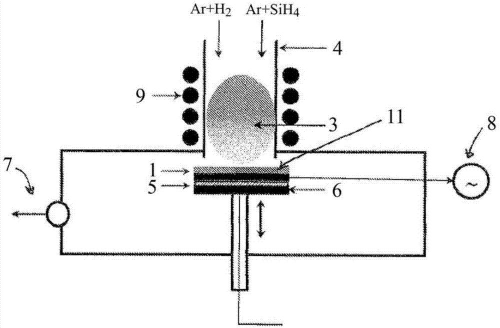
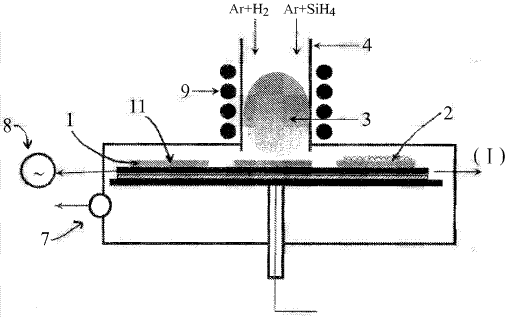
[0123] The thin silicon layers were obtained with an experimental setup consisting of a water-cooled stainless steel chamber, a cold cage plasma torch 4, and a substrate holder also water-cooled.

[0124] ( i) UMG silicon substrate

[0125] Substrate 1 is a UMG silicon substrate with a thickness of 400 μm and an average grain size of 8 mm. It includes metallic impurities at a level of 500ppb, boron at a level of 30ppm, and phosphorus at a level of 10ppm.

[0126] (ii) Thermal plasma chemical vapor deposition

[0127] The UMG silicon substrate was placed on a substrate holder equipped with a graphite resistance heating device 6 in order to reach a temperature of about 1100°C. The temperature is controlled using a thermocouple coupled to the generator.

[0128] The pressure of the chamber is reduced to 1 mbar by means of a suction device 7 . At this pressure, a plasma discharge was initiated by a radio frequency generator operating at a frequency of 4 MHz and a power of ...


PUM

PropertyMeasurementUnit
particle sizeaaaaaaaaaa
thicknessaaaaaaaaaa

Abstract

The invention relates to a method for forming a crystallised silicon layer (2) having a crystallite size higher than or equal to 100 µm, by means of epitaxial growth in a vapour phase, on the surface of at least one silicon substrate (1), comprising at least the steps consisting in: (i) providing a silicon substrate (1) having a particle size higher than or equal to 100 µm and comprising a metal impurities content of between 0 ppb and 1 ppm by weight; and (ii) forming said silicon layer on the surface of said substrate heated to a temperature of between 1000 and 1300 °C, by decomposition of at least one silicon precursor by means of an inductive plasma torch (4), the surface (11) of said substrate for supporting the silicon layer (2) being positioned close to the outlet of the plasma torch in step (ii).

Description

technical field [0001] The present invention relates to a new process for forming high-quality silicon epitaxial layers having a grain size greater than or equal to 100 μm. Background technique [0002] The photovoltaic market is experiencing strong growth and diversification of applications. This continued growth makes it necessary to be able to reduce the production costs of solar cells, which are mainly produced with silicon. The conventional process consists in using approximately 200 μm thick silicon wafers as the basic support for the solar cells. [0003] The reduction in the manufacturing costs of photovoltaic cells includes reducing the consumption of silicon during the production of said cells. To do this, one solution consists in depositing a thin layer of silicon tens of microns thick on a mechanical support called a substrate. [0004] Much research has been done with the aim of producing such thin silicon layers for photovoltaic cells. For economical reason...

Claims


Application Information

Patent Timeline
Patent Type & Authority Applications(China)
IPC IPC(8): C30B23/02C30B23/06C30B25/10C30B25/18C30B25/20C30B28/14C30B29/06C23C16/24C23C16/513H01L21/205H01L31/18H01L21/02
CPCY02E10/547H01L21/02381H01L21/02532C30B25/18C23C16/513C30B25/16H01L31/1804C30B29/06C23C16/24H01L21/0262C30B25/20H01L21/02595C30B25/105H05H1/30Y02P70/50
Inventor 马利克·本曼索尔让-保罗·加朗代丹尼尔·莫尔万
Owner COMMISSARIAT A LENERGIE ATOMIQUE ET AUX ENERGIES ALTERNATIVES
Why Eureka
Try Eureka