Method for growing CdS film or CdS nano-structure on CdTe film

A nanostructure and thin film technology, applied in the field of solar cells, can solve the problems that have not been reported, and achieve the effect of increasing the utilization rate, simple equipment, and simplifying the preparation process

Active Publication Date: 2015-07-29
NANJING UNIV
View PDF4 Cites 1 Cited by
  • Summary
  • Abstract
  • Description
  • Claims
  • Application Information

AI Technical Summary

Problems solved by technology

[0005] As far as the applicant knows, the method of growing a CdS layer (film or nanostructure) in situ on the surface of a CdTe film to form a pn junction has not been reported

Method used


Image

  • Method for growing CdS film or CdS nano-structure on CdTe film
  • Method for growing CdS film or CdS nano-structure on CdTe film
  • Method for growing CdS film or CdS nano-structure on CdTe film

Examples


Embodiment

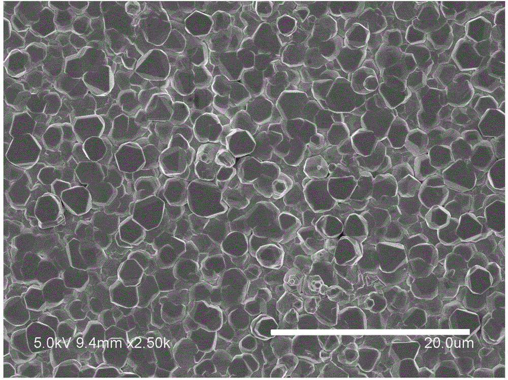
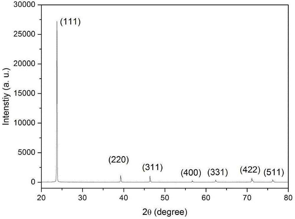
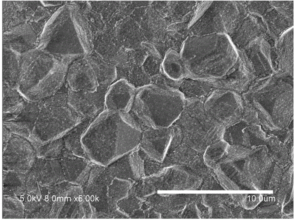
[0041] The above-mentioned prepared CdTe film is packed into a quartz tube, put into a sintering furnace, and sealed, and the quartz tube is evacuated with a vacuum pump. When the air pressure is reduced to 1Pa, the pumping is stopped, and after the hydrogen sulfide gas is introduced into the quartz tube, Seal; the sintering furnace is heated to 420°C at 10°C / min, and starts to cool down naturally after 60 minutes of heat preservation. After the temperature drops to room temperature, the film is taken out to obtain a finished product. like Figure 8 It can be seen from the figure that the phase structure of CdS is also formed after annealing in static hydrogen sulfide gas.

[0042] Example 4

[0043] The above-mentioned prepared CdTe film is packed into a quartz tube, put into a sintering furnace, and sealed, then feed 100 sccm of nitrogen to flush the quartz tube for 5 min, to get rid of the air in the quartz tube; then feed the mixed gas of nitrogen and hydrogen sulfide...


PUM

PropertyMeasurementUnit
thicknessaaaaaaaaaa
thicknessaaaaaaaaaa
thicknessaaaaaaaaaa

Abstract

The invention relates to a method for growing a CdS film or CdS nano-structure on a CdTe film. The method comprises the following steps of 1) filling the CdTe film into a quartz tube, and then placing the quartz tube into a sintering furnace to eliminate superfluous gas inside the quartz tube; 2) inletting mixed gas containing hydrogen sulfide, increasing the temperature of the sintering furnace to anneal the CdTe film; 3) performing cooling after the annealing step, discharging the film to obtain a finished product. According to the method for growing the CdS film or CdS nano-structure on the CdTe film, the CdTe film is placed inside the sintering furnace, the sintering furnace is filled with the hydrogen sulfide, then the temperature of the sintering furnace is increased, and lastly, the CdS film or CdS nano-structure can be formed in situ on the surface of the CdTe film. The method for growing the CdS film or CdS nano-structure on the CdTe film has the advantages of being simple in equipment and low in cost, and during a growing process, being low in temperature, saving catalyst and formworks and the like, and meanwhile, is a novel heterojunction preparing method and can be applied to preparation of heterostructural photovoltaic batteries such as CIGS, CZTS and CdTe.

Description

technical field [0001] The invention relates to the technical field of solar cells, in particular to a method for growing a CdS film or a CdS nanostructure on a CdTe film. Background technique [0002] At present, traditional energy sources such as coal and oil occupy a dominant position in our life, but they affect our daily life with high energy consumption and high pollution, and bring great disadvantages to our life. As a new energy source, solar energy has been valued by governments of various countries because of its inexhaustible, inexhaustible, and widely distributed advantages. [0003] CdTe-based photovoltaic solar cells are one of the second-generation new energy thin-film solar cells. Its core components are composed of p-type CdTe absorber layer and n-type CdS window layer. The absorber CdTe material is a direct bandgap semiconductor with a bandgap of 1.48 eV, which matches well with the solar spectrum. It has a high absorption coefficient, up to 10 5 cm -...

Claims


Application Information

Patent Timeline
Patent Type & Authority Applications(China)
IPC IPC(8): H01L21/02
CPCB82Y30/00B82Y40/00H01L21/02365
Inventor 马李刚刘文超吴小山张凤鸣
Owner NANJING UNIV
Why Eureka
Try Eureka