Ultraviolet semiconductor light-emitting device and manufacturing method thereof

A light-emitting device and semiconductor technology, applied in the field of optoelectronics, can solve problems such as difficult ohmic contact and lack of effective solutions, and achieve the effect of overcoming large surface resistance, high external quantum efficiency, and high reflectivity

Active Publication Date: 2017-07-07
NANJING UNIV
View PDF1 Cites 0 Cited by
  • Summary
  • Abstract
  • Description
  • Claims
  • Application Information

AI Technical Summary

Problems solved by technology

[0008] However, UV LEDs with flip-chip and vertical structures must use p-type ohmic contacts with high reflection and low resistance, so as to improve the light efficiency of the device, and the existing technology still lacks effective solutions
The significant decrease in the reflectivity of Ag in the ultraviolet band and the strong absorption of ultraviolet light by ITO are no longer suitable as p-type ohmic contact materials for UV LEDs with flip-chip and vertical structures. At the same time, metal Al, which has a high reflectivity in the ultraviolet band, Difficult to form a good ohmic contact with p-GaN or p-AlGaN

Method used


Image

  • Ultraviolet semiconductor light-emitting device and manufacturing method thereof
  • Ultraviolet semiconductor light-emitting device and manufacturing method thereof
  • Ultraviolet semiconductor light-emitting device and manufacturing method thereof

Examples


Embodiment 1

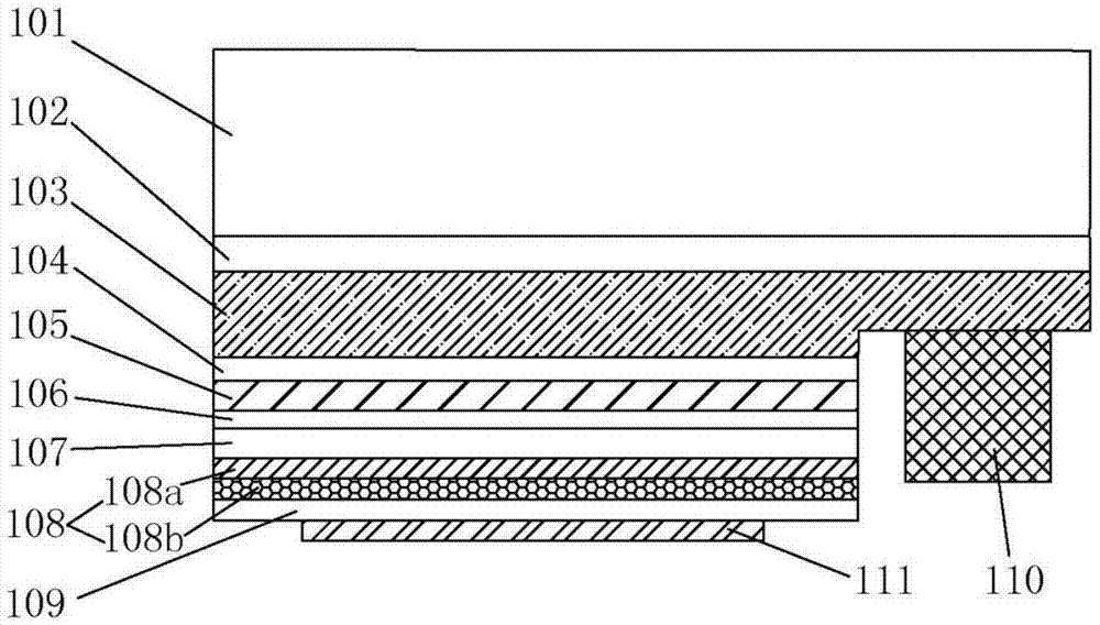
[0051]Embodiment 1 refers to figure 1 , the structure of the GaN-based ultraviolet LED chip is as follows from bottom to top: sapphire substrate 101, epitaxial layer including AlN buffer layer 102, n-AlGaN layer 103, n-AlGaN electron expansion layer 104, multiple quantum well layer 105, AlGaN Electron blocking layer 106, p-AlGaN layer 107, and graphene film cover Ag nano-dot layer 108 (wherein Ag nano-dot layer 108a, graphene film layer 108b), conductive reflection layer 109, n-type electrode 110, p-type electrode 111 .

[0052] The manufacturing steps of the GaN-based ultraviolet LED chip are described in detail below, which includes:

[0053] Step S1: On the sapphire substrate, use the MOCVD process to grow epitaxial layers in sequence. The epitaxial layers include a GaN buffer layer with a thickness of about 2.0 μm, an n-AlGaN layer with a thickness of about 2.0 μm, and an n-AlGaN electron expansion layer with a thickness of about 200 nm. layer, an InGaN / AlGaN multiple qu...

Embodiment 2

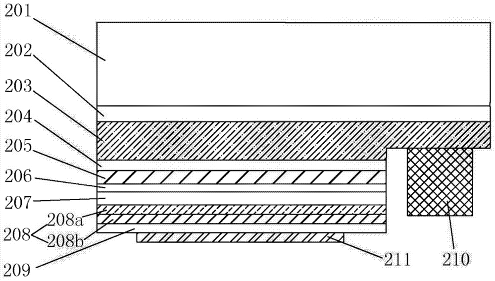
[0062] Embodiment 2 refers to figure 2 The structure of the GaN-based ultraviolet LED chip is as follows from bottom to top: a silicon carbide substrate 201, and the epitaxial layer includes an AlN buffer layer 202, an n-AlGaN layer 203, an n-AlGaN electron expansion layer 204, a multi-quantum well layer 205, p-AlGaN electron blocking layer 206, p-GaN layer 207, and coated graphene quantum dots loaded Ag nanoparticles layer 208 (graphene quantum dots loaded Ag nanoparticles composite layer 208a, intermediate layer 208b), conductive reflective layer 209 , n-type electrode 210, p-type electrode 211.

[0063] The manufacturing steps of the GaN-based ultraviolet LED chip are described in detail below, which includes:

[0064] Step S1: The purified graphene quantum dots and silver nitrate mixed solution are heated and refluxed to prepare the graphene quantum dots loaded Ag nanoparticle complex (reference "Synthesis of Silver Nanoparticles Supported onGraphene Quantum Dots for Oxy...

Embodiment 3

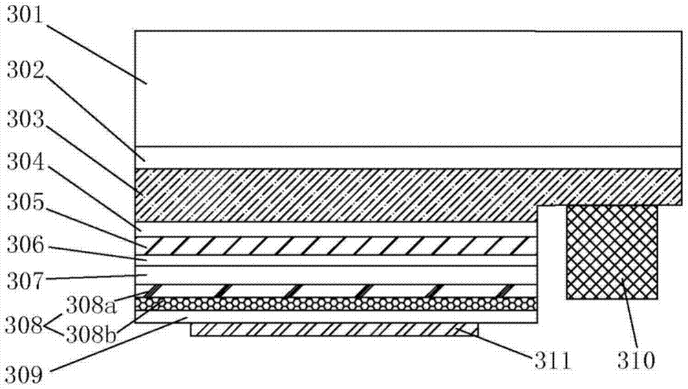
[0070] Embodiment 3 refers to figure 1 , the structure of the GaN-based ultraviolet LED chip is as follows from bottom to top: sapphire substrate 301, epitaxial layer including AlN buffer layer 302, n-AlGaN layer 303, n-AlGaN electron expansion layer 304, multiple quantum well layer 305, AlGaN Electron blocking layer 306, p-AlGaN layer 307, graphene film covering silver nanowire layer 308 (Ag nanowire layer 308a, graphene film layer 308b), conductive reflection layer 309, n-type electrode 310, p-type electrode 311.

[0071] The manufacturing steps of the GaN-based ultraviolet LED chip are described in detail below, which includes:

[0072] Step S1: On the sapphire substrate, use the MOCVD process to grow epitaxial layers in sequence. The epitaxial layers include an AlN buffer layer with a thickness of about 2.0 μm, an n-AlGaN layer with a thickness of about 2.0 μm, and an n-AlGaN electron expansion layer with a thickness of about 200 nm. layer, an InGaN / AlGaN multiple quantum...


PUM

PropertyMeasurementUnit
particle diameteraaaaaaaaaa
diameteraaaaaaaaaa
lengthaaaaaaaaaa

Abstract

The invention discloses an ultraviolet semiconductor light emitting device and a manufacturing method thereof. The device comprises an epitaxial layer composed of an n-type layer, a quantum well layer and a p-type layer, a p-type electrode and an n-type electrode. The p-type layer is further provided with a graphene-Ag nanocomposite layer and a conductive reflecting layer sequentially, and the graphene-Ag nanocomposite layer and the p-type layer are in ohmic contact. Furthermore, the graphene-Ag nanocomposite layer includes an Ag nano material layer formed on the p-type layer, and the Ag nano material layer comprises Ag nano points and / or Ag nano lines and a graphene film covering the Ag nano material layer; or, graphene quantum points load an Ag nanoparticle composite layer. The device has the advantages of high external quantum efficiency, high light emitting efficiency, low start voltage, fine heat radiation and high stability, the manufacturing process is simple and controllable, cost is low, and the device is adaptive to industrial production.

Description

technical field [0001] The invention relates to a semiconductor light-emitting element, in particular to an ultraviolet semiconductor light-emitting device and a manufacturing method thereof. The semiconductor light-emitting device can be used in fields such as transportation, medical treatment, display and white light illumination, and belongs to the field of optoelectronic technology. Background technique [0002] GaN-based ultraviolet / deep ultraviolet light-emitting diodes (LEDs) have the potential advantages of small size, long life, high efficiency, environmental protection, and energy saving, and they can replace existing ones in industrial curing, disinfection, water purification, medical and biochemistry, and high-density optical recording. There are ultraviolet light sources such as mercury lamps and gas lasers, which have important application prospects and broad market demands. [0003] LED chips are usually divided into front-mount, flip-chip and vertical structu...

Claims


Application Information

Patent Timeline
Patent Type & Authority Patents(China)
IPC IPC(8): H01L33/40H01L33/00
CPCH01L33/0066H01L33/0075H01L33/40H01L33/405H01L33/46H01L2933/0016H01L2933/0025
Inventor 周玉刚余显正张荣
Owner NANJING UNIV
Why Eureka
Try Eureka