Epitaxial wafer structure for flip LED chips and making method thereof

A technology of LED chips and manufacturing methods, which is applied in the direction of electrical components, circuits, semiconductor devices, etc., can solve the problems of unclean etching of deep grooves, unsatisfactory etching uniformity, and increased chip manufacturing costs, etc. Effects of quantum efficiency, improvement of internal quantum efficiency, and improvement of light extraction efficiency

Active Publication Date: 2015-08-12
HANGZHOU SILAN AZURE
View PDF3 Cites 2 Cited by
  • Summary
  • Abstract
  • Description
  • Claims
  • Application Information

AI Technical Summary

Problems solved by technology

[0004] The high-voltage LED chip structure is generally formed after the epitaxial layer is formed, and the isolation groove is formed by photolithography, and then the isolation groove is filled with insulating material, and finally electrodes are made on each insulated and separated epitaxial layer to form a series structure; although this The structure can improve the luminous brightness of the LED, but the process of forming the isolation groove and filling the insulating material greatly increases the manufacturing cost of the chip. Not only that, but also reduces the reliability of the LED chip to a certain extent. For example, due to the existing etching If the uniformity does not meet the requirements, the deep groove etching is not clean, which will eventually lead to leakage and reduce the breakdown resistance of the LED chip, etc.
[0005] Although the vertical LED chip structure does not need to etch the N-region material, it reduces a part of the production cost of the LED to a certain extent, and is suitable for high-current injection, which can further improve the luminous brightness of the LED chip. However, like the high-voltage chip, the vertical Structured LEDs also need to form isolation grooves, which greatly increases the production cost of LEDs. Not only that, vertical structure chips also need to peel off the growth substrate, which again increases the production cost of LED chips and reduces the cost of LED chips. yield and reliability
[0006] The f

Method used


Image

  • Epitaxial wafer structure for flip LED chips and making method thereof
  • Epitaxial wafer structure for flip LED chips and making method thereof
  • Epitaxial wafer structure for flip LED chips and making method thereof

Examples


Embodiment 1

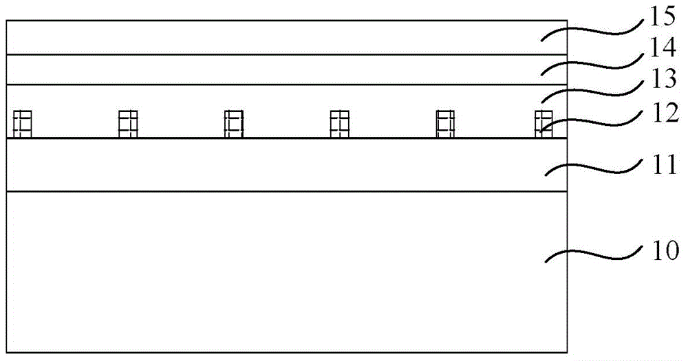
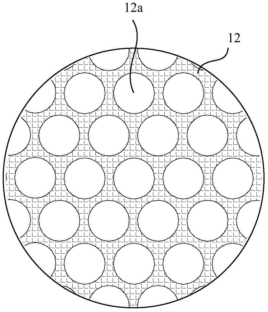
[0034] figure 1 It is a cross-sectional view of the epitaxial wafer structure for flip-chip LED chips according to Embodiment 1 of the present invention, figure 2 It is a top view of the communication medium layer in Embodiment 1 of the present invention;

[0035] Such as figure 1 and figure 2As shown, the epitaxial wafer structure for flip-chip LED chips includes a supporting substrate 10, a lattice matching layer 11, a communication medium layer 12 with periodically arranged columnar structures 12a, an N-type semiconductor layer 13, The active layer 14 and the P-type semiconductor layer 15, the lattice matching layer 11 is formed on the support substrate 10, the communication medium layer 12 is formed on the lattice matching layer 11 and exposes part of the A lattice matching layer 11, the N-type semiconductor layer 13 covers the communication medium layer 12 and the lattice matching layer 11, the crystal structure of the lattice matching layer 11 is the same as the cry...

Embodiment 2

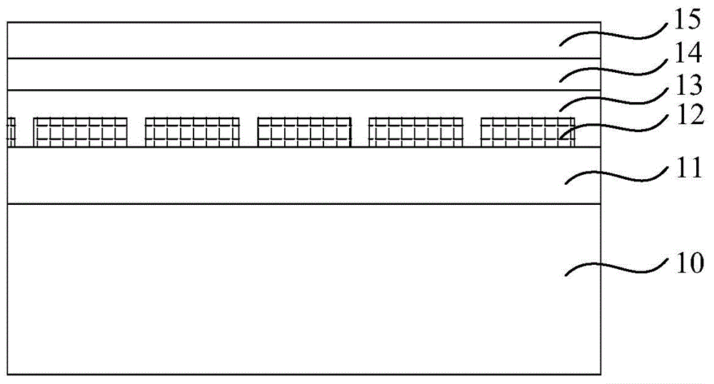
[0048] image 3 It is a cross-sectional view of the epitaxial wafer structure for flip-chip LED chips according to Embodiment 2 of the present invention, Figure 4 It is a top view of the communication medium layer in Embodiment 2 of the present invention.

[0049] Such as image 3 and Figure 4 As shown, the difference between this embodiment and Embodiment 1 is that the columnar structure 12a is a columnar protrusion, and the communication medium layer 12 is composed of periodically arranged columnar protrusions, and the crystals are exposed through the gaps between the columnar protrusions. Lattice matching layer 11.

[0050] More specifically, the columnar structure 12a is a cylindrical protrusion. Of course, since the supporting substrate 10 is a circular substrate, the columnar structures 12a on the edge of the supporting substrate 10 may be incomplete cylindrical protrusions, and the present invention does not impose any restrictions on the number and arrangement of...

Embodiment 3

[0052] The difference between this embodiment and the first embodiment is that the columnar structure 12a is a polygonal columnar protrusion. Figure 5 It is a top view of the communication medium layer in Embodiment 3 of the present invention. Such as Figure 5 As shown, the columnar structure 12a in this embodiment is a hexagonal prism protrusion.


PUM


Abstract

The invention provides an epitaxial wafer structure for flip LED chips and a making method thereof. The epitaxial wafer structure for flip LED chips comprises a support substrate, a lattice matching layer, a connecting dielectric layer, an N-type semiconductor layer, an active layer and a P-type semiconductor layer, all of which are formed sequentially, wherein the connecting dielectric layer is provided with periodically arranged columnar structures. The connecting dielectric layer provided with periodically arranged columnar structures exposes part of the lattice matching layer. The N-type semiconductor layer covers the connecting dielectric layer provided with periodically arranged columnar structures and the lattice matching layer. The epitaxial wafer structure and the making method thereof are conductive to increasing the internal quantum efficiency and the external quantum efficiency of flip LED chips.

Description

technical field [0001] The invention belongs to the field of semiconductor optoelectronic chip manufacturing, and in particular relates to an epitaxial wafer structure for flip-chip LED chips and a manufacturing method thereof. Background technique [0002] Since the commercialization of GaN-based LEDs in the early 1990s, after more than 20 years of development, its structure has become mature and perfect, and it has been able to meet people's current needs for lighting decoration; but it must completely replace traditional light sources and enter the lighting industry. In the field of lighting, especially in the field of high-end lighting, the improvement of luminous brightness is the never-ending pursuit of scientific researchers in the LED industry. In recent years, the most active technology in improving LED luminance is undoubtedly the patterned substrate technology. The patterned substrate technology not only improves the crystal quality of LED epitaxy by reducing latt...

Claims


Application Information

Patent Timeline
IPC IPC(8): H01L33/12H01L33/22H01L33/00
CPCH01L33/007H01L33/12H01L33/22
Inventor 张昊翔丁海生李东昇赵进超黄捷陈善麟江忠永
Owner HANGZHOU SILAN AZURE
Why Eureka
Try Eureka