A kind of ge-sb-te-se film material for phase change memory and its preparation method
A phase-change memory and thin-film material technology, applied in the direction of electrical components, etc., can solve the problems of low thermal stability, high melting point, and excessive RESET current in the amorphous state, and achieve the effects of simple manufacturing process, long cycle life, and improved performance
- Summary
- Abstract
- Description
- Claims
- Application Information
AI Technical Summary
Problems solved by technology
Method used
Image
Examples
Embodiment 1
[0028] A Ge-Sb-Te-Se thin film material for phase change memory, which is a material composed of germanium-antimony-tellurium-selenium four elements, wherein antimony and tellurium can form Sb-Sb and Sb- Te stable phase, the two phases composite at the nanoscale, can be composed similarly to GeTe and Sb 2 Te 3 pseudo-binary system.
Embodiment 2
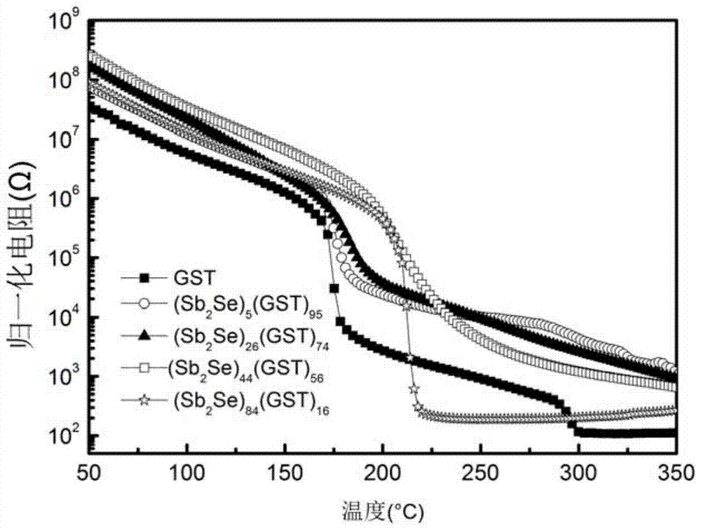
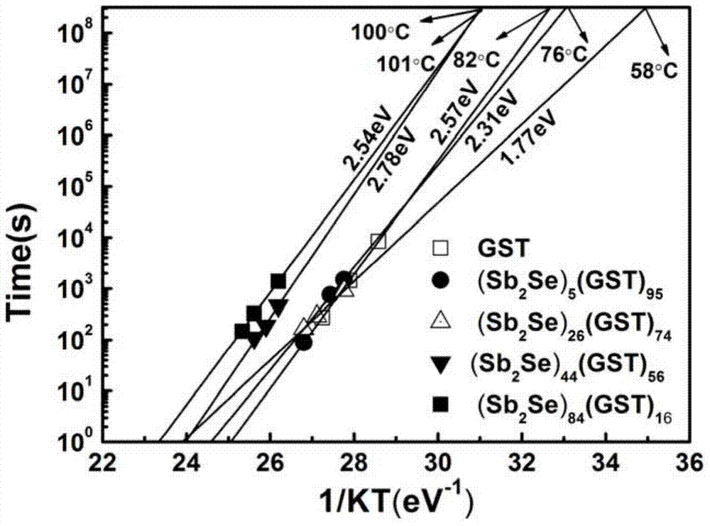
[0030] A kind of Ge-Sb-Te-Se film material for phase change memory, the chemical structural formula of this film material is (Sb 2 Se) x(Ge 2 Sb 2 Te 5 ) y , where Sb 2 The overall molar percentage of Se is 0%2 Sb 2 Te 5 The overall molar percentage is 16%≤y%≤95%, x+y=100, which specifically includes the following steps:
[0031] (1) In the magnetron sputtering coating system, Sb 2 Se targets and Ge 2 Sb 2 Te 5 The targets are respectively installed in the magnetron radio frequency sputtering target, and the semiconductor is used as the substrate;
[0032] (2) Vacuumize the sputtering chamber of the magnetron sputtering coating system until the vacuum degree in the chamber reaches 1.6×10 -4 Pa, and then feed high-purity argon into the sputtering chamber until the pressure in the sputtering chamber reaches 0.3 Pa for the initiation pressure required for sputtering;
[0033] (3) Then control the power of the RF power supply on the Sb2Se target to 3-13W, and the Ge ...
Embodiment 3
[0035] With above-mentioned embodiment 2, its difference is: in the preparation process alloy Sb 2 The sputtering power of the Se target was controlled to 0W, and the Ge 2 Sb 2 Te 5 The sputtering power of the target is controlled to 40W, and Ge 2 Sb 2 Te 5 Phase change memory thin film material.
PUM
| Property | Measurement | Unit |
|---|---|---|
| crystallization temperature | aaaaa | aaaaa |
Abstract
Description
Claims
Application Information


