GaN high electron mobility transistor (HEMT) technology based monolithic integration active quasi circulator

A monolithic integration and circulator technology, which is applied to amplifiers with semiconductor devices/discharge tubes, amplifiers, waveguide devices, etc., can solve the problems of unbearable power amplifier power and small power capacity, and achieve convenient system or module Design, large power capacity, and reduced system area

Active Publication Date: 2015-08-26
NANJING UNIV OF SCI & TECH
View PDF1 Cites 17 Cited by
  • Summary
  • Abstract
  • Description
  • Claims
  • Application Information

AI Technical Summary

Problems solved by technology

[0003] In active circulators based on microwave monolithic integrated circuits (MMICs), complementary metal-oxide-semiconductor (CMOS) processes are widely used because of lower power loss, but as document 1 (H.S.Wu, C.W.Wang, and C.K.C. Tzuang, "CMOS active quasi-circulator with dual transmission gains incorporating feedforward technique at K-band," IEEE Trans. Microw. Theory Tech., vol.58, no.8, pp.2084–2091, Aug.2010.) and literature 2 (D.Huang, J.Kuo, and H.Wang, "A24-GHz low power and high isolation active quasi-circulator," 2012IEEE MTT-S International Microwave Symposium Digest, Montreal, Canada, Jun.2012, pp .1–3.), the power capacity of the active circulator based on the CMOS process is generally small at the 1dB compression point, and the circulator is usually located after the power amplifier, so it will not be able to be used in high-power applications such as T / R modules. Withstands power at the output of the power amplifier

Method used


Image

  • GaN high electron mobility transistor (HEMT) technology based monolithic integration active quasi circulator
  • GaN high electron mobility transistor (HEMT) technology based monolithic integration active quasi circulator
  • GaN high electron mobility transistor (HEMT) technology based monolithic integration active quasi circulator

Examples


Embodiment 1

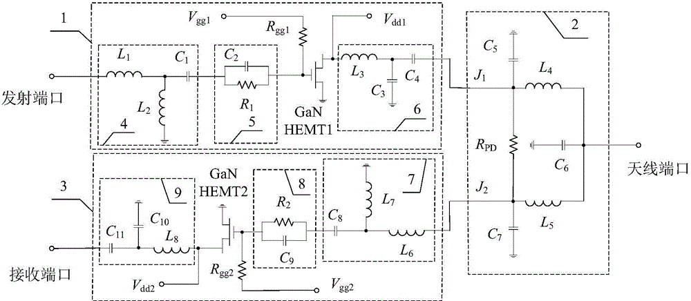
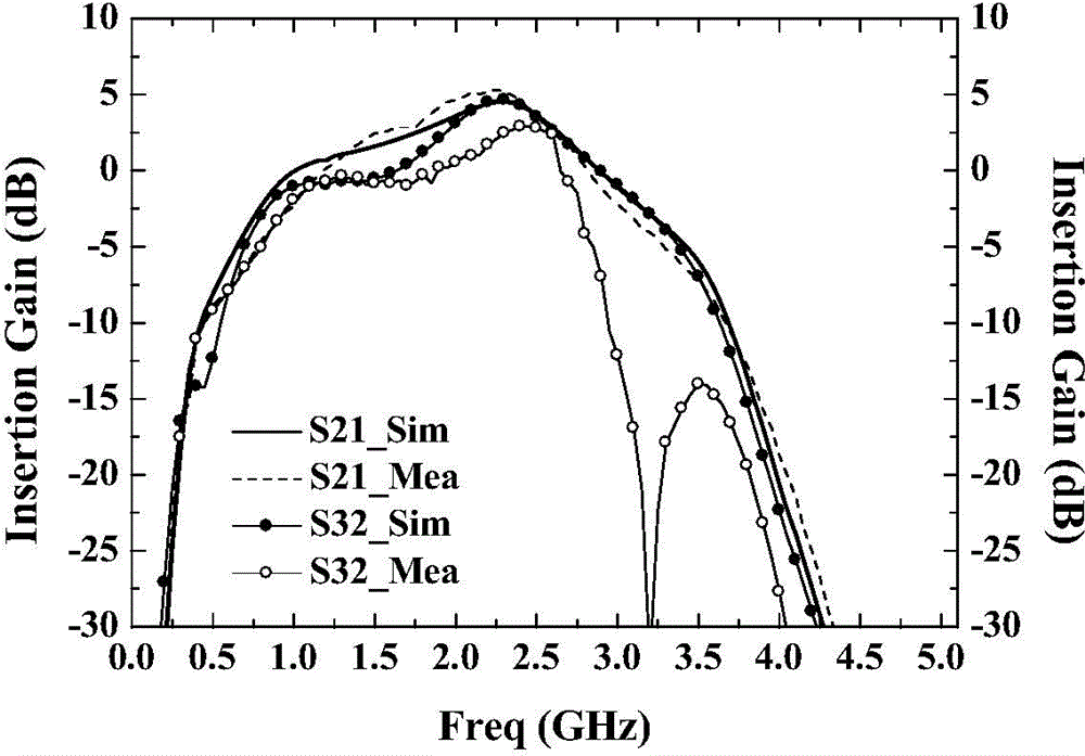
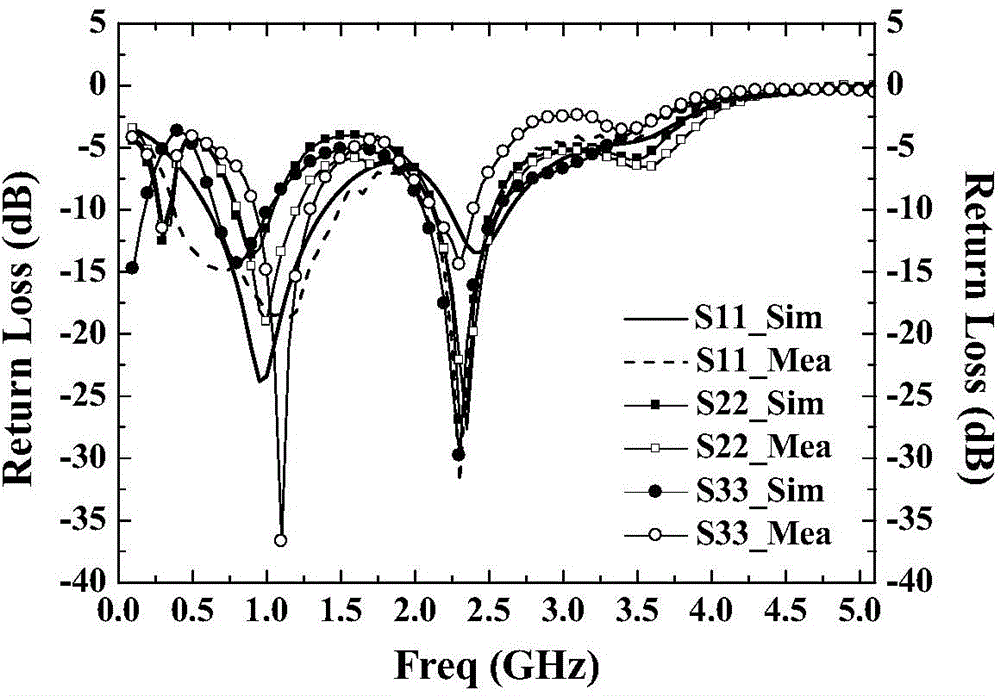
[0035] In this embodiment, the monolithic integrated active quasi-circulator based on the GaN HEMT process has an overall monolithic circuit size of 2.5mm×1.5mm, and the isolation resistor R in the lumped power divider 2 PD Using a 100-ohm thin film resistor, the MMIC lumped inductance in the lumped power divider 2 and the fourth inductance L 4 and the fifth inductance L 5 The size is 4.83nH, the fifth capacitor C of the MMIC lumped capacitor 5 and the sixth capacitor C 6 The size is 1.15pF, the seventh capacitor C 7 The size is 2.16pF.

[0036] The total gate width of the GaN HEMT in the power amplifier of this embodiment is 8×100 μm, and a conjugate matching design is adopted between the power amplifier and the power divider to realize maximum power transmission. In terms of DC bias circuit design, TFR resistors are used in the DC bias circuit of the gate of the amplifier, and the voltage is directly applied to the first grid bias input terminal V through a DC probe. gg...


PUM


Abstract

The invention discloses a GaN high electron mobility transistor (HEMT) technology based monolithic integration active quasi circulator. The monolithic integration active quasi circulator comprises a transmitting branch power amplifier, a lumped power divider and a receiving branch power amplifier, which are sequentially connected and are integrated in the same chip through an AlGaN / GaN HEMT technology. The transmitting branch power amplifier, from a transmitting port, comprises a first input match circuit, a first stabilizing circuit, a first gallium nitride transistor and a first output match circuit, which are sequentially connected. An output end of the first output match circuit is connected with a first power dividing port J1 of the lumped power divider. A synthesis port of the lumped power divider is an antenna port. The structure of the receiving branch power amplifier is the same as the structure of the transmitting branch power amplifier. A second power dividing port J1 of the lumped power divider is used as an input end. An output end of the receiving branch power amplifier is a receiving port of the active quasi circulator. The monolithic integration active quasi circulator effectively reduces circuit area, has large power capacity, and has a broad application prospect.

Description

technical field [0001] The invention belongs to the technical field of microwave single-chip integrated circuits, in particular to a single-chip integrated active quasi-circulator based on GaN HEMT technology. Background technique [0002] In the transceiver components of the microwave and millimeter wave systems of the continuous wave system, the circulator is a three-port non-reciprocal device, which can enable an antenna to simultaneously receive and transmit signals, effectively reducing the area of ​​the transceiver system. Passive circulators are generally made of ferrite materials, which have the advantages of low insertion loss, small power loss, high stability, and large power capacity, but their volume is too large, their bandwidth is relatively narrow, and it is difficult to use them in a single chip. Integrated design, so it cannot adapt to the needs of integration and miniaturization of today's communication systems. So active circulators designed using bipolar...

Claims


Application Information

Patent Timeline
Patent Type & Authority Applications(China)
IPC IPC(8): H03F3/195H03F3/24H01P1/38
Inventor 车文荃顾黎明蔡奇陈海东冯文杰
Owner NANJING UNIV OF SCI & TECH
Why Eureka
Try Eureka