Schottky diode and manufacturing method thereof

A technology of Schottky diode and manufacturing method, applied in semiconductor/solid-state device manufacturing, electrical components, circuits, etc., can solve the problems of low forward turn-on voltage, small on-resistance, and high breakdown voltage, and achieve forward turn-on The effect of low voltage, low on-resistance and high breakdown voltage

Active Publication Date: 2015-09-02
GPOWER SEMICON
View PDF4 Cites 9 Cited by
  • Summary
  • Abstract
  • Description
  • Claims
  • Application Information

AI Technical Summary

Problems solved by technology

[0006] The object of the present invention is to propose a Schottky diode and a manufacturing method thereof. The Schottky diode can solve the problem that the Schottky diode in the prior art cannot simultaneously have small reverse leakage, high breakdown voltage, and forward opening. The problem of low voltage and small on-resistance

Method used


Image

  • Schottky diode and manufacturing method thereof
  • Schottky diode and manufacturing method thereof
  • Schottky diode and manufacturing method thereof

Examples


Embodiment 1

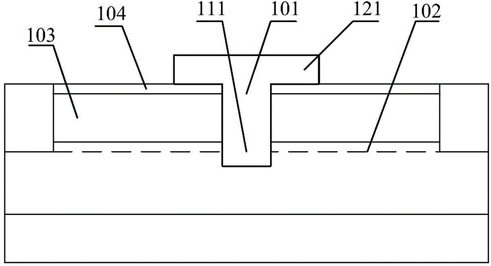
[0059] image 3 is a schematic cross-sectional view of the Schottky diode provided by Embodiment 1 of the present invention. Such as image 3 shown, the Schottky diode consists of:

[0060] Substrate 1. Among them, the material of the substrate 1 can be silicon carbide, silicon nitride, silicon, sapphire, aluminum nitride, gallium nitride, SOI (silicon-on-insulator, Silicon-On-Insulator) or other epitaxial growth III- Substrate material for Group V nitrides. Among them, SOI technology introduces a buried oxide layer between the top silicon and the back substrate.

[0061] Preferably, a nucleation layer 2 and a buffer layer 3 are sequentially deposited on the substrate 1 . Among them, the material of the nucleation layer 2 can be aluminum nitride, gallium nitride or other III-V nitrides; the material of the buffer layer 3 can be non-doped aluminum nitride, gallium nitride, aluminum gallium nitride or other III - Group V nitrides.

[0062] The first semiconductor layer 4 ...

Embodiment 2

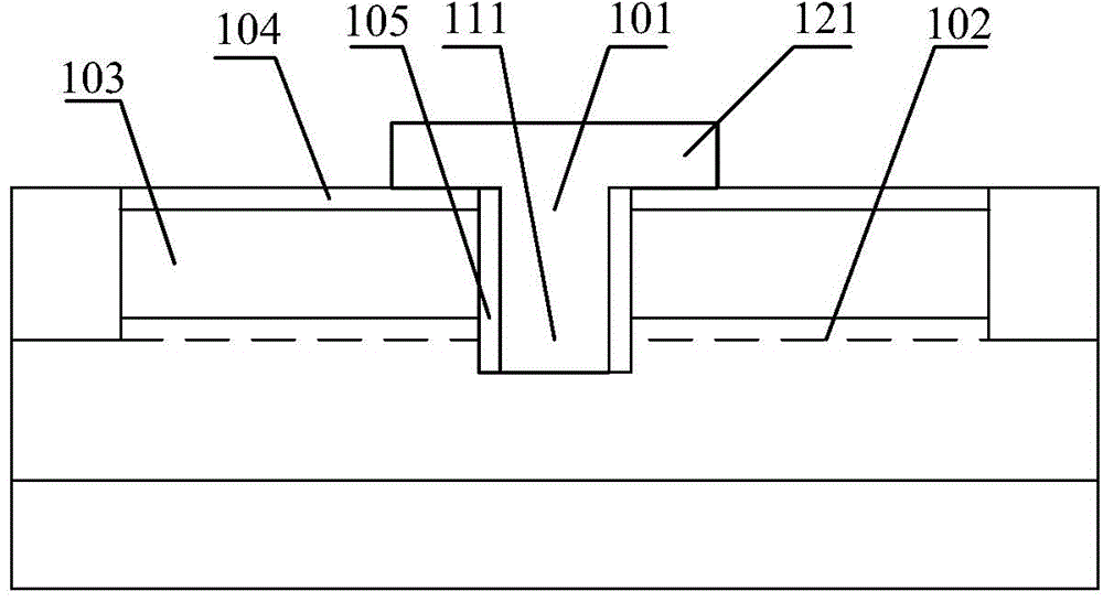
[0073] Figure 6 is a schematic cross-sectional view of the Schottky diode provided by Embodiment 2 of the present invention. Such as Figure 6 As shown, the difference from the Schottky diode provided in Embodiment 1 is that the high work function anode 10 of the Schottky diode provided in Embodiment 2 extends to the upper surface of the first passivation dielectric layer 7 to form an anode field board structure.

[0074] Compared with the Schottky diode provided in Embodiment 1 of the present invention, the Schottky diode provided in Embodiment 2 of the present invention has an anode field plate structure, which can further reduce the peak electric field at the edge of the anode, thereby reducing the Schottky junction Leakage.

Embodiment 3

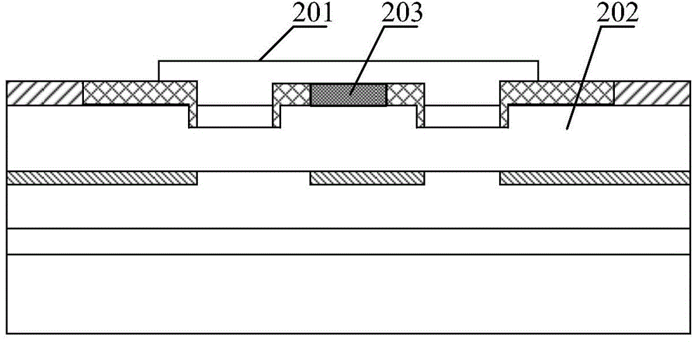
[0076] Figure 7 is a schematic cross-sectional view of the Schottky diode provided in Embodiment 3 of the present invention. Such as Figure 7 As shown, the difference from the Schottky diode provided in Embodiment 2 is that the Schottky diode provided in Embodiment 3 also includes:

[0077] The field plate groove in the first passivation medium layer 7 is located under the high work function anode 10 , the bottom of the field plate groove is located on the upper surface of the second semiconductor layer 5 , and the high work function anode 10 covers the field plate groove. Wherein, the shape of the side surface of the field plate groove section is: straight line, broken line or arc; the angle between any side surface of the field plate groove and the bottom surface of the field plate groove is: right angle, obtuse angle or acute angle.

[0078] Compared with the Schottky diode provided in Embodiment 2 of the present invention, the anode structure of the Schottky diode prov...


PUM


Abstract

The invention discloses a Schottky diode and a manufacturing method thereof. The Schottky diode comprises a substrate, a first semiconductor layer, a second semiconductor layer, a first passivation dielectric layer, a cathode, an anode slot, a low work function anode and a high work function anode, wherein the first semiconductor layer is located on the substrate; the second semiconductor layer is located on the first semiconductor layer, and a two-dimensional electron gas is formed at the at the interface between the first semiconductor layer and the second semiconductor layer; the first passivation dielectric layer is located on the second semiconductor layer, and a part of the second semiconductor layer is exposed out of the first passivation dielectric layer; the cathode is arranged on the exposed part of the second semiconductor layer or extends to the upper surface of the first passivation dielectric layer; the anode slot extends from the first passivation dielectric layer to a region where the two-dimensional electron gas is positioned or exceeds the region where the two-dimensional electron gas is positioned; the low work function anode is arranged on the anode slot and extends to the upper surface of the second semiconductor layer; and the high work function anode covers the low work function anode, and is electrically connected with the low work function anode. The Schottky diode provided by the invention has the advantages of being low in reverse electric leakage, high in breakdown voltage, low in forward threshold voltage and turn-on resistance.

Description

technical field [0001] The invention relates to the field of semiconductors, in particular to a Schottky diode and a manufacturing method thereof. Background technique [0002] In the application field of high-voltage switches, it is hoped that the diode has the characteristics of small reverse leakage, large reverse withstand voltage and small forward conduction voltage drop. Power electronic devices based on wide-bandgap semiconductor materials, especially gallium nitride materials, have superior properties. Therefore, Gallium Nitride Schottky diodes have gradually become a research hotspot in recent years. [0003] At present, Schottky diodes based on AlGaN / GaN heterostructures have gradually become an important research direction in the industry. But existing AlGaN / GaN Schottky diodes still have deficiencies. For example, field thermal electron emission or electron tunneling effect under high electric field will increase the reverse leakage, resulting in a decrease in...

Claims


Application Information

Patent Timeline
Patent Type & Authority Applications(China)
IPC IPC(8): H01L29/872H01L29/417H01L21/28H01L21/329
CPCH01L29/417H01L29/66143H01L29/872
Inventor 张乃千赵树峰陈洪维
Owner GPOWER SEMICON
Why Eureka
Try Eureka