Surface treatment method and texturing method for diamond wire cutting silicon wafers

A diamond wire, surface treatment technology, applied in the direction of final product manufacturing, sustainable manufacturing/processing, semiconductor/solid-state device manufacturing, etc., to achieve the effect of improving conversion efficiency

Active Publication Date: 2015-09-09
JIA XING SHANGNENG PHOTOVOLTAIC MATERIALS SCI & TECH CO LTD
View PDF4 Cites 28 Cited by
  • Summary
  • Abstract
  • Description
  • Claims
  • Application Information

AI Technical Summary

Problems solved by technology

[0006] In view of this, in order to solve the existing deficiencies, the present invention provides a surface treatment method and a texturing method of a diamond wire-cut silicon wafer, which are used for subsequent use of conventional texturing processes for HNO 3 The / HF system creates conditions for effective texturing of silicon wafers, thus solving the problem of texturing silicon wafers by diamond wire cutting

Method used


Image

  • Surface treatment method and texturing method for diamond wire cutting silicon wafers
  • Surface treatment method and texturing method for diamond wire cutting silicon wafers
  • Surface treatment method and texturing method for diamond wire cutting silicon wafers

Examples


Embodiment 1

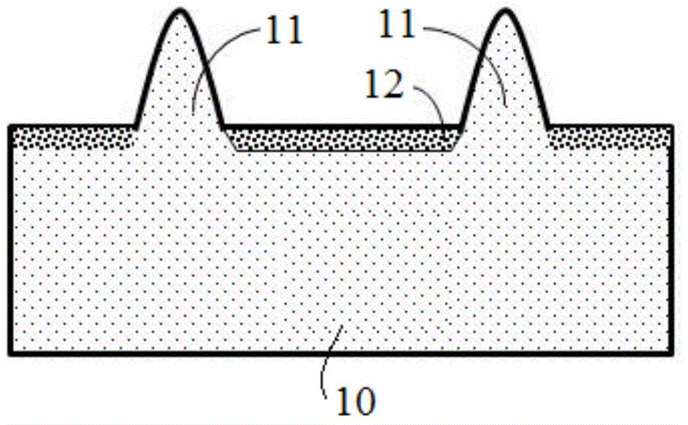
[0069] A surface treatment method for diamond wire-cut silicon wafers, such as Figure 1a-1d shown, including the following steps:

[0070] (1) Put a diamond wire-cut silicon wafer with a thickness of 180±10 μm and a size of 156mm×156mm into 4% HF solution for 240s to remove SiO on the surface 2 oxide layer; then put into deionized water and ultrasonically clean for 120s; wherein, the diamond wire-cut silicon wafer in this embodiment can be a diamond wire-cut monocrystalline silicon wafer or a diamond wire-cut polycrystalline silicon wafer;

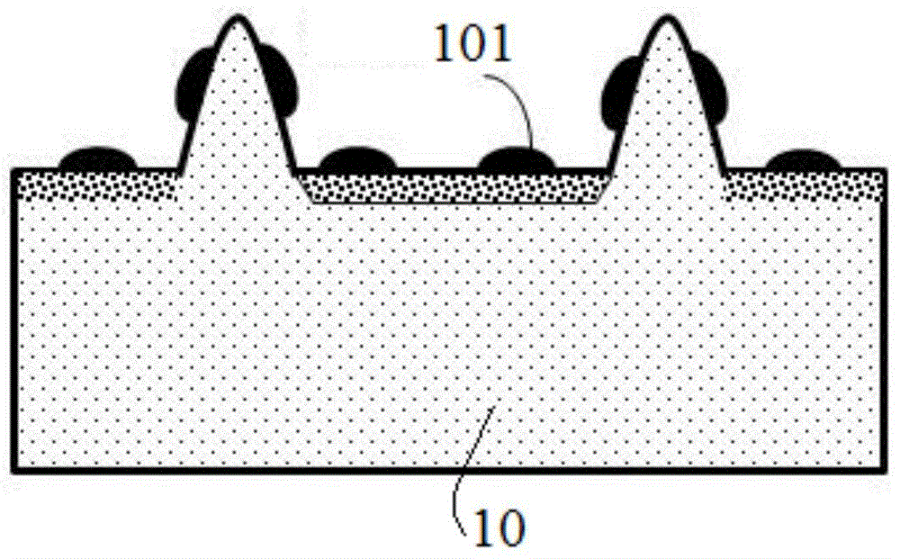
[0071] (2) Put the silicon wafer after the previous step into the silicon wafer containing Ag ions, HF, H 2 o 2 In the mixed aqueous solution, the concentrations are 0.005mol / L, 3mol / L, and 0.1mol / L respectively, and react at 25°C for 60s;

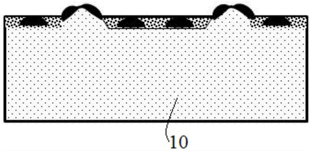
[0072] (3) Putting the silicon chip after the previous step into a 69% nitric acid solution by mass and cleaning it for 300 s, the cleaning temperature is 25° C.;

[0073] (4) Put the silicon wafer...

Embodiment 2

[0082] A surface treatment method for diamond wire-cut silicon wafers, such as Figure 1a-1d shown, including the following steps:

[0083] (1) Put a diamond wire-cut silicon wafer with a thickness of 180±10 μm and a size of 156mm×156mm into 4% HF solution for 240s to remove SiO on the surface 2 oxide layer; then put into deionized water and ultrasonically clean for 120s; wherein, the diamond wire-cut silicon wafer in this embodiment can be a diamond wire-cut monocrystalline silicon wafer or a diamond wire-cut polycrystalline silicon wafer;

[0084] (2) Put the silicon wafer after the previous step into the silicon wafer containing Cu ions, HF, H 2 o 2 In the mixed aqueous solution, the concentrations are 0.01mol / L, 3mol / L, and 0.1mol / L respectively, and react at 30°C for 60s;

[0085] (3) Putting the silicon chip after the previous step into a 69% nitric acid solution by mass and cleaning it for 300 s, the cleaning temperature is 25° C.;

[0086] (4) Put the silicon wafer ...


PUM

PropertyMeasurementUnit
thicknessaaaaaaaaaa
heightaaaaaaaaaa

Abstract

The invention discloses a surface treatment method and a texturing method for diamond wire cutting silicon wafers. The surface of a diamond wire cutting silicon wafer is covered with an amorphous silicon layer caused by cutting, and line marks are densely distributed on the surface of the diamond wire cutting silicon wafer. The surface treatment method comprises the following steps: cleaning and pre-treating a diamond wire cutting silicon wafer; putting the cleaned and pre-treated diamond wire cutting silicon wafer in mixed solution containing metal ions, oxidizing agent and etching agent, and carrying out metal ion adhesion, SiO2 generation through oxidation, and catalytic chemical etching reaction in sequence; cleaning the etched silicon wafer with first cleaning fluid, second cleaning fluid and deionized water respectively, and removing metal particles, an oxide layer and chemical residues on the surface of the silicon wafer; and cleaning the silicon wafer to obtain a silicon wafer which has no line marks and contains a micro-defect amorphous layer. According to the invention, a diamond wire cutting silicon wafer can be effectively textured through a regular process, and the conversion efficiency of a crystalline silicon solar cell prepared with the textured silicon wafer is improved.

Description

technical field [0001] The invention relates to the technical field of crystalline silicon surface treatment, in particular to a surface treatment method and a texturing method of a diamond wire-cut silicon wafer. Background technique [0002] At present, most of the cutting of monocrystalline and polycrystalline silicon wafers used in solar silicon cells adopts the silicon carbide mortar multi-wire cutting technology, that is, the silicon carbide particles in the mortar are driven by high-speed moving steel wires to be rolled and ground to cut silicon wafers; the disadvantages of this technology include Low slicing efficiency, need to use chemical coolant, large kerf leads to small number of slicing per unit mass, expensive silicon carbide abrasives and a large amount of silicon powder produced by cutting are difficult to separate and recycle, etc. The new diamond wire cutting technology is to fix the diamond on the steel wire, and cut the silicon wafer by scraping the shar...

Claims


Application Information

Patent Timeline
Patent Type & Authority Applications(China)
IPC IPC(8): H01L21/306H01L21/02H01L31/18
CPCH01L21/02052H01L21/30604H01L31/1804H01L31/182Y02E10/546Y02E10/547Y02P70/50
Inventor 苏晓东叶晓亚
Owner JIA XING SHANGNENG PHOTOVOLTAIC MATERIALS SCI & TECH CO LTD
Why Eureka
Try Eureka