High-temperature wave absorbing metamaterial and preparation method thereof
A metamaterial and high-temperature technology, applied in chemical instruments and methods, electrical components, layered products, etc., can solve the problems of poor low-frequency absorption performance, low absorption efficiency, poor designability, etc., and achieve good microwave absorption performance and simple structure , the performance is easy to adjust the effect
- Summary
- Abstract
- Description
- Claims
- Application Information
AI Technical Summary
Problems solved by technology
Method used
Image

Examples
Embodiment 1
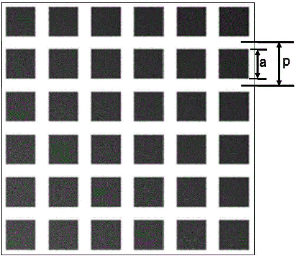
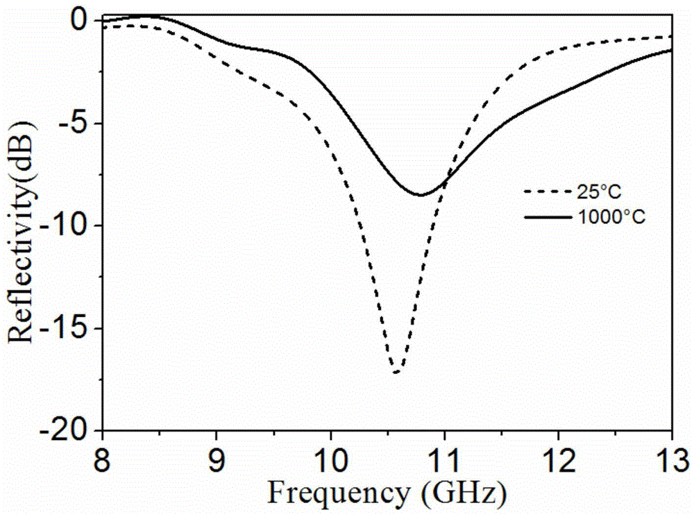
[0027] Titanium diboride ceramic powder was prepared by self-propagating high-temperature synthesis method, and then dense titanium diboride ceramics with a certain thickness were prepared by hot-pressing sintering method, and titanium diboride ceramics were cut into thicknesses of 0.5 mm, a square sheet with a side length a of 5 mm. The aluminum oxide dielectric substrate and the cut titanium diboride ceramic sheet are subjected to ultrasonic surface treatment in ethanol to ensure that the surface to be bonded is clean and free of oil, and then dried in an oven. The titanium diboride ceramic sheets are periodically bonded on the alumina dielectric substrate with an inorganic high-temperature adhesive, and are periodically arranged to form a conductive ceramic array, and then the other side of the alumina dielectric substrate and the reflective backplane are passed through an inorganic high-temperature For adhesive connection, heat at 30°C for 1.5 hours, then raise the tempera...
Embodiment 2
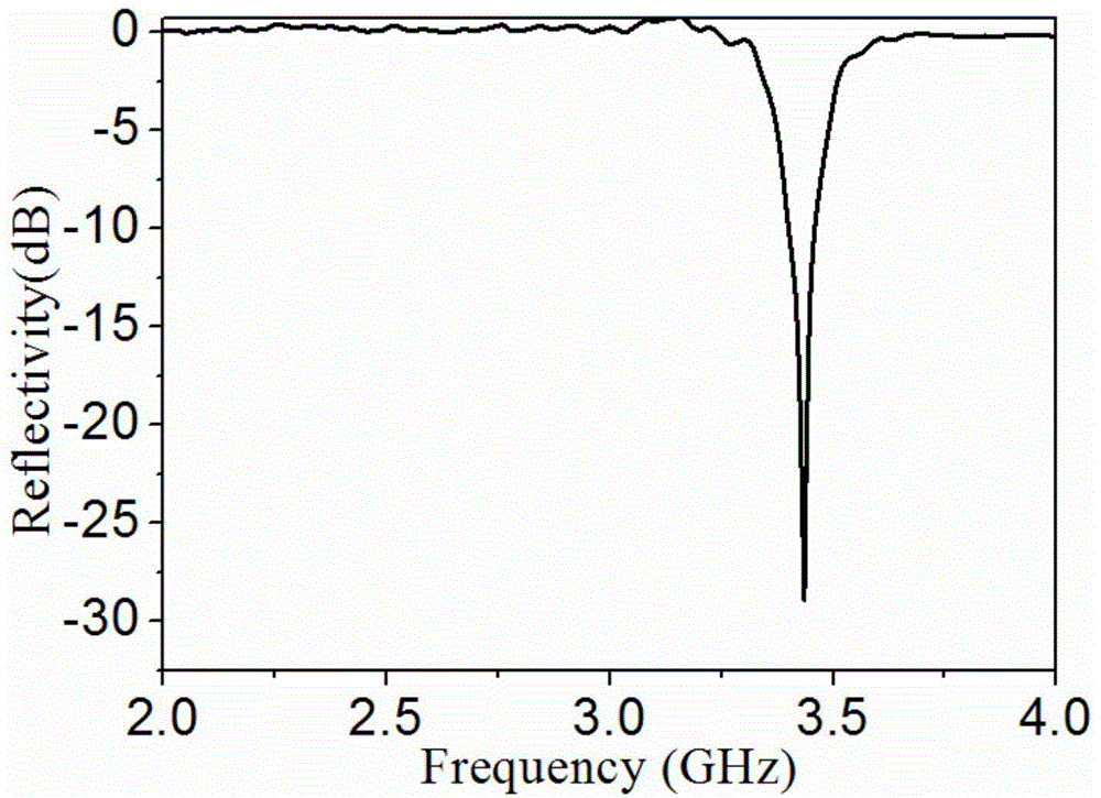
[0029] Titanium diboride ceramic powder was prepared by self-propagating high-temperature synthesis method, and then dense titanium diboride ceramics with a certain thickness were prepared by hot-pressing sintering method, and titanium diboride ceramics were cut into thicknesses of 0.5 mm, a square sheet with a side length a of 15mm. The aluminum oxide dielectric substrate and the cut titanium diboride ceramic sheet are subjected to ultrasonic surface treatment in ethanol to ensure that the surface to be bonded is clean and free of oil, and then dried in an oven. The titanium diboride ceramic sheets are periodically bonded on the alumina dielectric substrate with an inorganic high-temperature adhesive, and are periodically arranged to form a conductive ceramic array, and then the other side of the alumina dielectric substrate and the reflective backplane are passed through an inorganic high-temperature For adhesive connection, heat at 35°C for 1.5 hours, then raise the tempera...
Embodiment 3
[0031] Titanium diboride ceramic powder was prepared by self-propagating high-temperature synthesis method, and then dense titanium diboride ceramics with a certain thickness were prepared by hot-pressing sintering method, and titanium diboride ceramics were cut into thicknesses of 0.5 About mm, the square sheet whose side lengths are a=5mm and b=6mm respectively. The silicon carbide / silicon nitride composite ceramic dielectric substrate and the cut titanium diboride ceramic sheet are subjected to ultrasonic surface treatment in ethanol to ensure that the surface to be bonded is clean and free of oil, and then dried in an oven. Use an inorganic high-temperature adhesive to periodically bond titanium diboride ceramic flakes on a silicon carbide / silicon nitride composite ceramic dielectric substrate, and form a periodic arrangement to form a conductive ceramic array, and then place the silicon carbide / silicon nitride composite ceramic The other side of the dielectric substrate i...
PUM
| Property | Measurement | Unit |
|---|---|---|
| Reflectivity | aaaaa | aaaaa |
| Reflectivity | aaaaa | aaaaa |
| Reflectivity | aaaaa | aaaaa |
Abstract
Description
Claims
Application Information