An oxide thin film transistor, array substrate and display device

A technology of oxide thin films and transistors, which is applied in the direction of transistors, electric solid-state devices, semiconductor devices, etc., can solve the problems of low mobility and poor stability, and achieve the effect of improving TFT mobility and carrier concentration

Active Publication Date: 2018-07-31
BOE TECH GRP CO LTD
View PDF5 Cites 0 Cited by
  • Summary
  • Abstract
  • Description
  • Claims
  • Application Information

AI Technical Summary

Problems solved by technology

[0004] The invention provides an oxide thin film transistor, an array substrate and a display device to solve the technical problems of poor stability and low mobility of the oxide thin film transistor in the prior art

Method used


Image

  • An oxide thin film transistor, array substrate and display device
  • An oxide thin film transistor, array substrate and display device
  • An oxide thin film transistor, array substrate and display device

Examples


Embodiment 1

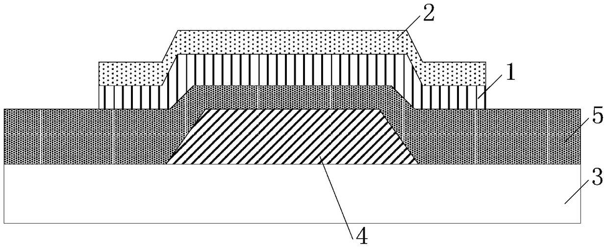
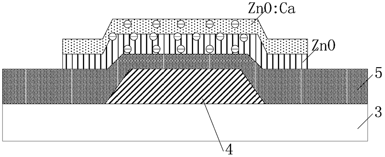
[0042] Embodiment 1 of the present invention provides an oxide thin film transistor, which is a ZnO system TFT with a bottom gate structure. The back channel oxide layer 2 is an ion-doped ZnO system with a large band gap, and the front channel oxide layer 1 is an ion-doped or non-ion-doped ZnO system with a small band gap.

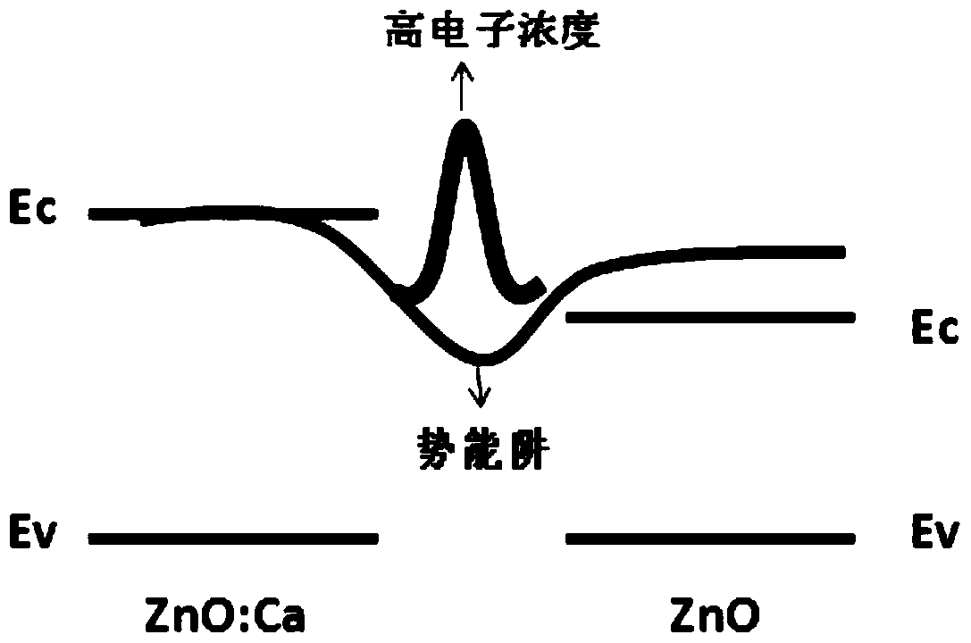
[0043] Among them, a front channel oxide layer 1 is deposited on the gate insulating layer 5, which is a ZnO system material, and then a back channel oxide layer 2 formed by a low work function ion-doped ZnO system material is deposited, marked as ZnO: M, where M represents doped metal ions, which can be Ca with low work function 2+ or Mg 2+ and other metal ions. In this embodiment 1, metal Ca is exemplified 2+ , recorded as ZnO: Ca.

[0044] The ZnO system material in this embodiment 1 can be ZnO or ion-doped zinc oxide system material, such as: IGZO, ITZO and other materials. Among them, since the bandgap (Eg) of calcium oxide CaO is 7.1eV, and the ...

Embodiment 2

[0049] Embodiment 2 of the present invention provides an oxide thin film transistor, and the materials of the back channel oxide layer 2 and the front channel oxide layer 1 are different.

[0050] Among them, the front channel oxide layer 1 is deposited on the gate insulating layer 5, and a ZnO system material with a small forbidden band width and a low conduction band energy level is deposited on this layer, and the forbidden band width of the ZnO system is ~ 3eV; then ZrO is deposited. 3 System material, ZrO 3 The bandgap width of ~5.5eV, due to ZnO and ZrO 3 The conduction band energy level difference and the forbidden band width difference, electrons are composed of ZrO 3 transfer to ZnO, and in ZrO 3 / ZnO interface forms a potential energy well, see Figure 4 , the electron concentration accumulated in the potential energy well is the highest, and the interface potential energy well with the highest electron concentration becomes the main channel for electron transport...

Embodiment 3

[0053] Embodiment 3 of the present invention provides an array substrate, including the oxide thin film transistor described in any one of the above items.


PUM


Abstract

The embodiments of the present invention provides an oxide TFT, an array substrate and a display device, an oxide channel layer of the oxide TFT comprises a front channel oxide layer and a back channel oxide layer, a conduction band bottom of the back channel oxide layer being higher than a conduction band bottom of the front channel oxide layer, and a band gap of the back channel oxide layer being larger than a band gap of the front channel oxide layer. In the oxide TFT, the array substrate and the display device provided in the present invention, it is possible to accumulate a large number of electrons through the potential difference formed between oxide channel layers of a multilayer structure so as to increase the carrier concentration in the oxide channel layers to achieve the purpose of improving TFT mobility without damaging TFT stability.

Description

technical field [0001] The present invention relates to the field of display technology, in particular to an oxide thin film transistor, an array substrate and a display device. Background technique [0002] With the development of high image resolution, high refresh rate, 3D and other technologies, the development of high mobility TFT materials is very important. The mobility of low temperature polysilicon can be as high as 100cm 2 / Vs, but its preparation cost is high, and the uniformity needs to be further improved when producing large-size backplanes. At present, the oxide channel materials that have been studied more include indium gallium zinc oxide (IGZO), indium tin zinc oxide (ITZO) and other materials, and their mobility is between 10 and 30 cm 2 / Vs or so, it needs to be further improved in practical application. [0003] In the oxide TFT industry, it is common to increase the number of carriers in the channel by doping the oxide channel layer with metal ions t...

Claims


Application Information

Patent Timeline
Patent Type & Authority Patents(China)
IPC IPC(8): H01L29/786H01L29/10H01L27/12
CPCH01L29/7869H01L27/1225H01L29/10H01L29/1054H01L29/225H01L29/227H01L29/24H01L29/78696
Inventor 王美丽孙宏达刘凤娟辛龙宝
Owner BOE TECH GRP CO LTD
Why Eureka
Try Eureka