Organic electroluminescent light emitting device and preparation method thereof

An electroluminescent device, organic technology, applied in the direction of electric solid device, semiconductor/solid state device manufacturing, electrical components, etc., can solve the problem of low luminous efficiency of light emitting device

Inactive Publication Date: 2015-09-23
OCEANS KING LIGHTING SCI&TECH CO LTD +2
View PDF0 Cites 10 Cited by
  • Summary
  • Abstract
  • Description
  • Claims
  • Application Information

AI Technical Summary

Problems solved by technology

[0004] In traditional organic electroluminescent devices, the electron transport rate is two or three orders of magnitude lower than the hole transport rate. Therefore, the regi

Method used


Image

  • Organic electroluminescent light emitting device and preparation method thereof
  • Organic electroluminescent light emitting device and preparation method thereof
  • Organic electroluminescent light emitting device and preparation method thereof

Examples


preparation example Construction

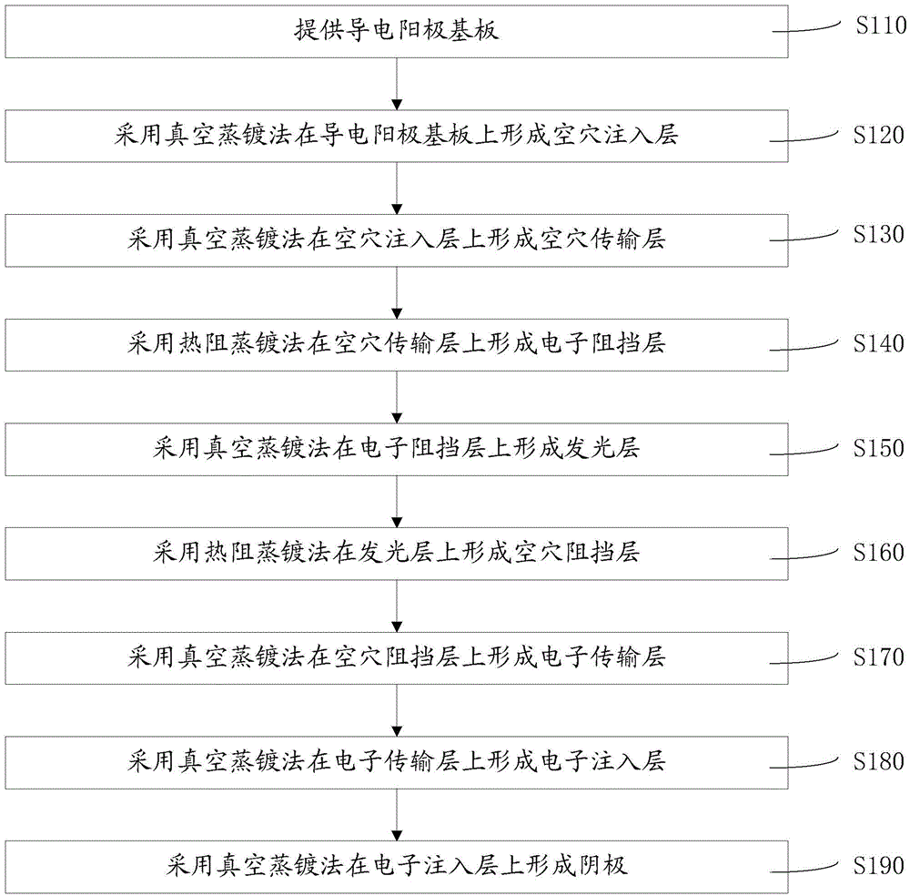
[0084] Such as figure 2 As shown, the method for preparing the above-mentioned organic electroluminescent device 100 according to an embodiment includes the following steps:

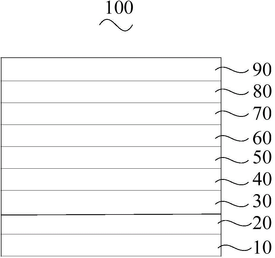
[0085] S110, providing a conductive anode substrate.

[0086] The conductive anode substrate 10 includes glass and a conductive anode film formed on one surface of the glass. The conductive anode film is indium tin oxide film (ITO), aluminum-doped zinc oxide film (AZO) or indium-doped zinc oxide film (IZO). The thickness of the conductive anode film is 50nm-300nm. Preferably, the conductive anode film is ITO with a thickness of 120nm.

[0087] The conductive anode film was prepared by magnetron sputtering. The acceleration voltage of magnetron sputtering is 300V-800V, the magnetic field is about 50G-200G, and the power density is 1W / cm 2 ~40W / cm 2 .

[0088] Before magnetron sputtering the conductive anode film, first rinse the glass with distilled water and ethanol, and soak it in isopropanol fo...

Embodiment 1

[0129] (1) After rinsing the glass with distilled water and ethanol, soak it in isopropanol overnight. A conductive anode film was prepared on one surface of the glass by magnetron sputtering. The acceleration voltage of magnetron sputtering is 700V, the magnetic field is 120G, and the power density is 25W / cm 2 . The material of the conductive anode film is ITO, and the thickness is 120nm.

[0130] (2) A hole injection layer is formed on the conductive anode substrate by vacuum evaporation method. The vacuum degree of vacuum evaporation is 8×10 -4 Pa, the evaporation rate is 0.2nm / s. The material of the hole injection layer is MoO 3 , with a thickness of 35nm.

[0131] (3) A hole transport layer is formed on the hole injection layer by a vacuum evaporation method. The vacuum degree of vacuum evaporation is 8×10 -4 Pa, the evaporation rate is 0.2nm / s. The material of the hole transport layer is NPB, and the thickness is 48nm.

[0132] (4) An electron blocking layer is...

Embodiment 2

[0141] (1) After rinsing the glass with distilled water and ethanol, soak it in isopropanol overnight. A conductive anode film was prepared on one surface of the glass by magnetron sputtering. The acceleration voltage of magnetron sputtering is 300V, the magnetic field is 50G, and the power density is 40W / cm 2 . The material of the conductive anode film is IZO with a thickness of 300nm.

[0142] (2) A hole injection layer is formed on the conductive anode substrate by vacuum evaporation method. The vacuum degree of vacuum evaporation is 2×10 -3 Pa, the evaporation rate is 1nm / s. The material of the hole injection layer is V 2 o 5 , with a thickness of 20nm.

[0143] (3) A hole transport layer is formed on the hole injection layer by a vacuum evaporation method. The vacuum degree of vacuum evaporation is 2×10 -3 Pa, the evaporation rate is 1nm / s. The material of the hole transport layer is TAPC, and the thickness is 50nm.

[0144] (4) An electron blocking layer is fo...


PUM

PropertyMeasurementUnit
Thicknessaaaaaaaaaa
Thicknessaaaaaaaaaa
Thicknessaaaaaaaaaa

Abstract

The invention provides an organic electroluminescent light emitting device which comprises a conductive anode substrate, a hole injection layer, a hole transmission layer, an electron blocking layer, a light emitting layer, a hole blocking layer, an electron transmission layer, an electron injection layer and a cathode which are stacked in order. The material of the electron blocking layer is a mixture of a first compound and a phosphorescent material. The first compound is a bipolar metal oxide, a lithium salt or a silicone small molecule. According to the organic electroluminescent light emitting device, the transmission rate of a hole can be improved by the electron blocking layer, electrons can be blocked at one side of electron blocking layer close to the light emitting layer, the hole can be blocked at one side of the hole blocking layer close to the light emitting layer by the hole blocking layer, thus the recombination area of excitons are controlled in the light emitting layer, and the light emitting efficiency of the organic electroluminescent light emitting device is improved. In addition, the invention also provides the preparation method of the organic electroluminescent light emitting device.

Description

technical field [0001] The invention relates to the technical field of electroluminescence, in particular to an organic electroluminescence device and a preparation method thereof. Background technique [0002] Organic Light-Emitting Diode (OLED) is a current-mode semiconductor light-emitting device based on organic materials. Its typical structure is to make a layer of tens of nanometers thick organic light-emitting material on the ITO glass as the light-emitting layer, and there is a metal electrode with a low work function above the light-emitting layer. When a voltage is applied to the electrodes, the light-emitting layer produces light radiation. [0003] In 1987, C.W.Tang and Van Slyke of Eastman Kodak Company in the United States reported a breakthrough in the research of organic electroluminescence. A high-brightness, high-efficiency double-layer organic electroluminescent device is prepared by using ultra-thin film technology. Brightness up to 1000cd / m at 10V 2 ...

Claims


Application Information

Patent Timeline
IPC IPC(8): H01L51/50H01L51/54H01L51/56
Inventor 周明杰黄辉张振华王平
Owner OCEANS KING LIGHTING SCI&TECH CO LTD
Why Eureka
Try Eureka