Vacuum sputtering electrode of ceramic thermistor and manufacturing method thereof
A thermistor and vacuum sputtering technology, which is applied in the direction of resistance terminals/electrodes, resistors with positive temperature coefficients, sputtering plating, etc., can solve problems such as unstable electrical properties, and achieve good consistency and low cost, effect of good electrical conductivity
- Summary
- Abstract
- Description
- Claims
- Application Information
AI Technical Summary
Problems solved by technology
Method used
Image
Examples
Embodiment 1
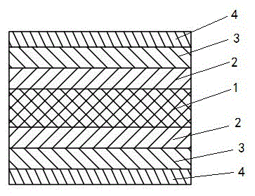
[0024] combine figure 1 , the ceramic thermistor vacuum sputtering electrode that the present embodiment relates to, its transition layer 2, barrier layer 3 and conductive layer 4 sputtered successively on the substrate 1 surface, wherein transition layer 2 is the nickel-chromium alloy of thickness 4000nm, In the nickel-chromium alloy, nickel is 80% by mass percentage, the barrier layer 3 is nickel-copper alloy with a thickness of 4000nm, in the nickel-copper alloy, nickel is 25% by mass percentage, and the conductive layer 4 is silver with a thickness of 2000nm.
[0025] The specific manufacturing process of the ceramic thermistor is as follows. After batching, wet ball milling, pre-firing, secondary wet ball milling, granulation, molding, and sintering, the sputtered substrate 1 is obtained, and the outer dimension of the substrate 1 is Φ8. 75×2.7mm. Since the surface state of the substrate 1 has a great influence on the adhesion, contamination on the surface of the substra...
Embodiment 2
[0027] Ceramic thermistor vacuum sputtering electrode, the transition layer, barrier layer and conductive layer sputtered successively on the surface of the substrate, wherein the transition layer is a nickel-chromium alloy with a thickness of 4500nm, and in the nickel-chromium alloy by mass percentage, nickel is 81%, the barrier layer is a nickel-copper alloy with a thickness of 4500nm, in the nickel-copper alloy, nickel is 29%, and the conductive layer is silver with a thickness of 2500nm. Its manufacture process is with embodiment 1.
Embodiment 3
[0029] Ceramic thermistor vacuum sputtering electrode, the transition layer, barrier layer and conductive layer sputtered successively on the surface of the substrate, wherein the transition layer is a nickel-chromium alloy with a thickness of 5000nm, and in the nickel-chromium alloy by mass percentage, nickel is 85%, the barrier layer is a nickel-copper alloy with a thickness of 5000nm, in the nickel-copper alloy, nickel is 30%, and the conductive layer is silver with a thickness of 3000nm. Its manufacture process is with embodiment 1.
PUM
| Property | Measurement | Unit |
|---|---|---|
| Thickness | aaaaa | aaaaa |
| Thickness | aaaaa | aaaaa |
| Thickness | aaaaa | aaaaa |
Abstract
Description
Claims
Application Information

