Polysilicon floating gate memory based on organic field effect transistor and its preparation method

A technology of polysilicon and organic fields, which is applied in transistors, semiconductor/solid-state device manufacturing, semiconductor devices, etc., can solve the problems of high operating voltage and high manufacturing cost, and achieve the effects of reducing operating voltage, improving retention characteristics, and increasing mobility

Inactive Publication Date: 2018-11-16
LANZHOU UNIVERSITY
View PDF1 Cites 0 Cited by
  • Summary
  • Abstract
  • Description
  • Claims
  • Application Information

AI Technical Summary

Problems solved by technology

[0005] The purpose of the present invention is to provide a polysilicon floating gate memory based on an organic field effect transistor and a preparation method thereof, so as to solve the problems of high operating voltage and high manufacturing cost of the existing organic field effect transistor floating gate memory

Method used


Image

  • Polysilicon floating gate memory based on organic field effect transistor and its preparation method
  • Polysilicon floating gate memory based on organic field effect transistor and its preparation method
  • Polysilicon floating gate memory based on organic field effect transistor and its preparation method

Examples


Embodiment Construction

[0030] The present invention will be described in detail below in combination with specific embodiments.

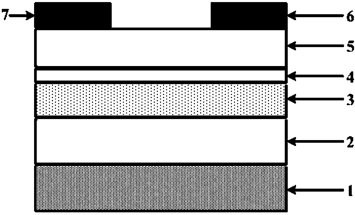
[0031] The structure of the polysilicon floating gate memory based on the organic field effect transistor of the present invention is as figure 1 As shown, its preparation process is as follows:

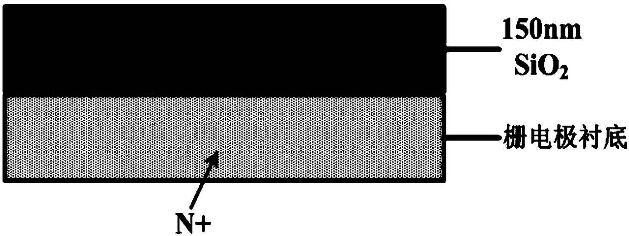
[0032] 1) Put the cleaned heavily doped silicon wafer into a thermal oxidation furnace, and thermally oxidize and grow a layer of SiO with a thickness of about 150-300nm on the silicon surface. 2 Thin layer, forming the gate insulating dielectric layer 2 of the device, such as figure 2 .

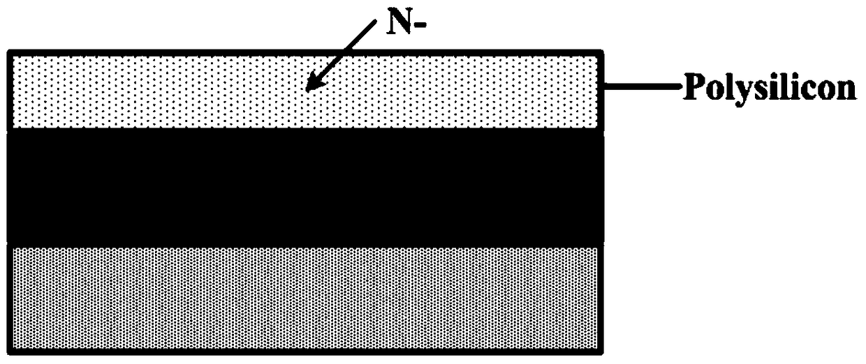
[0033] 2) Using CVD method, on SiO 2 A polysilicon layer with a thickness of 20-40nm (deposition rate of about 5nm / min) grown on the surface is used as the floating gate 3 of the device, such as image 3 .

[0034] 3) Using the ion implantation method, perform low-concentration arsenic ion doping in the polysilicon floating gate region (the doping concentration is about 10 16 / cm 3 ). ...


PUM


Abstract

The invention discloses a polysilicon floating gate memory based on an organic field effect transistor and a preparation method thereof. The gate electrode adopts a heavily doped low-resistance single crystal silicon substrate with a thickness of 100-300nm; the gate insulation formed on the surface of the gate electrode silicon substrate dielectric layer; a polysilicon floating gate embedded between the gate insulating dielectric layer and the tunneling insulating dielectric layer as a charge storage unit; a tunneling insulating dielectric layer formed on the surface of the floating gate; growing an organic semiconductor on the surface of the tunneling insulating dielectric layer material to form the active layer of the device; on the surface of the active layer, metal is vacuum-evaporated through a metal mask to form the source and drain of the device. The beneficial effect of the invention is to reduce the working voltage of the floating gate memory based on the organic field effect transistor, realize high-density storage of the device, improve the retention characteristic of the device, and reduce the manufacturing cost of the device.

Description

technical field [0001] The invention belongs to the technical field of electronic components, and relates to a polysilicon floating gate memory based on an organic field effect transistor and a preparation method thereof. Background technique [0002] With the continuous development of electronic information technology, electronic information products have gradually penetrated into every aspect of people's life, work and study. People's demand for low-cost, low-power, portable and miniaturized electronic devices is increasing. The traditional silicon-based It is difficult for non-volatile memory to meet the above new requirements. Organic floating gate memory is a new type of organic electronic device developed based on organic thin film field effect transistor. Attention is a new type of electronic device with very promising application prospects in the future. [0003] The structure of organic floating gate memory is similar to that of organic field effect transistors (OF...

Claims


Application Information

Patent Timeline
Patent Type & Authority Patents(China)
IPC IPC(8): H01L29/788H01L21/336H01L29/04H01L51/05
CPCH01L29/04H01L29/66825H01L29/788H10K10/00
Inventor 杨建红闫兆文肖彤谌文杰杨盼乔坚栗王娇
Owner LANZHOU UNIVERSITY
Why Eureka
Try Eureka