UTB-SOI tunneling field effect transistor with abrupt tunnel junction and preparation method

A UTB-SOI, tunneling field effect technology, applied in semiconductor/solid-state device manufacturing, semiconductor devices, electrical components, etc., can solve the problems of small driving current, sub-threshold slope theoretical value degradation, etc., to improve performance, suppress dual Extreme effect, high practical value effect

Inactive Publication Date: 2015-12-02
XIAN UNIV OF SCI & TECH
View PDF4 Cites 0 Cited by
  • Summary
  • Abstract
  • Description
  • Claims
  • Application Information

AI Technical Summary

Problems solved by technology

[0005] In order to overcome the problems of low driving current of existing silicon-based TFET devices and the degradation of subthreshold slope relative to the theoretical value, the present invention proposes a UTB-SOI tunneling field effect transistor with abrupt tunneling junction and its preparation method

Method used


Image

  • UTB-SOI tunneling field effect transistor with abrupt tunnel junction and preparation method
  • UTB-SOI tunneling field effect transistor with abrupt tunnel junction and preparation method
  • UTB-SOI tunneling field effect transistor with abrupt tunnel junction and preparation method

Examples


Embodiment 1

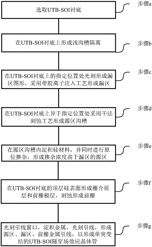
[0046] See figure 1 , figure 1 It is a flowchart of a method for preparing a UTB-SOI tunneling field effect transistor with an abrupt tunnel junction according to an embodiment of the present invention, and the method includes the following steps:

[0047] Step a, select UTB-SOI substrate;

[0048] Step b, forming shallow trench isolation on the UTB-SOI substrate;

[0049] Step c, photolithographically forming a drain region pattern at a specified position on the UTB-SOI substrate, and forming a drain region by using an ion implantation process with glue;

[0050] Step d, forming source region trenches on the UTB-SOI substrate at positions different from the designated positions by dry etching;

[0051] Step e, depositing silicon material in the trench of the source region, and performing in-situ doping at the same time, forming a source region with a higher doping concentration than the drain region;

[0052] Step f, forming a gate dielectric layer and a front gate layer ...

Embodiment 2

[0076] See Figure 2a-Figure 2h It is a schematic diagram of a method for preparing a UTB-SOI tunneling field-effect transistor with an abrupt tunneling junction according to an embodiment of the present invention; this embodiment takes the preparation of a UTB-SOI tunneling field-effect transistor with an abrupt tunneling junction as an example to illustrate, Specific steps are as follows:

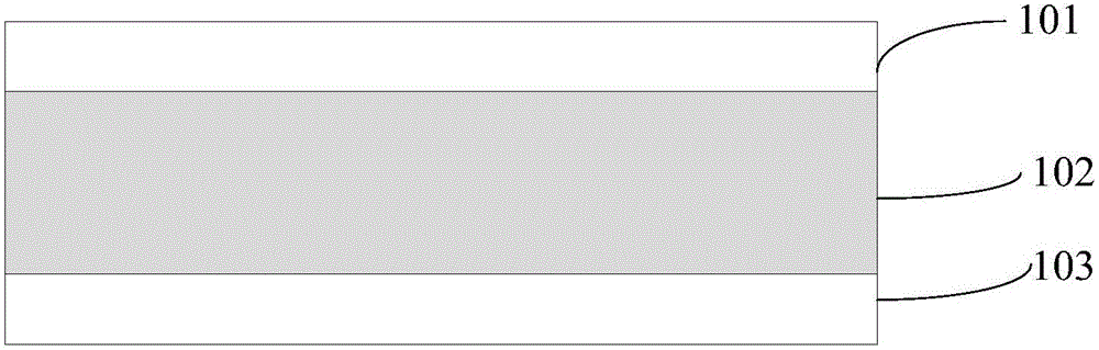
[0077] (1) Select the UTB-SOI substrate. Such as Figure 2a As shown, the UTB-SOI substrate includes a top layer of silicon 101 , a buried oxide layer 102 such as a buried layer of silicon dioxide, and a bottom layer of silicon 103 . The reason for using the UTB-SOI substrate is that the semiconductor device formed on the UTB-SOI substrate has low power consumption, high speed, high integration density, strong anti-interference ability, strong anti-radiation ability, simple process, and can completely eliminate the bulk The advantages of the parasitic latch-up effect of Si devices can ...

Embodiment 3

[0105] See image 3 , image 3 It is a schematic flow chart of a method for preparing a UTB-SOI tunneling field effect transistor with an abrupt tunneling junction according to an embodiment of the present invention, so as to prepare an N-type UTB-SOI tunneling field effect transistor with an abrupt tunneling junction with a channel length of 45 nm. Taking the transistor as an example to describe in detail, the specific steps are as follows:

[0106] 1. Select UTB-SOI substrate

[0107] The crystal orientation of the UTB-SOI substrate 101 may be (100) or (110) or (111), without any limitation here. In addition, the doping type of the UTB-SOI substrate 101 may be N type, or It can be P-type, and the doping concentration is, for example, 10 14 ~10 17 cm -3 , the thickness of the top layer Si is, for example, 10-20 nm.

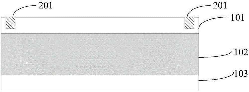
[0108] 2. Shallow trench isolation formation

[0109] 2.1 Form a first protective layer on the UTB-SOI substrate.

[0110] First, two layers of materials...


PUM


Abstract

The invention relates to an ultra-thin-body-silicon-on-insulator (UTB-SOI) tunneling field-effect transistor with an abrupt tunneling junction and a preparation method. The preparation method comprises: selecting a UTB-SOI substrate; forming a shallow trench isolation unit; carrying out photoetching to form a drain region graph and carrying out adhesive ion implantation to form a drain region; carrying out dry etching to form a source region trench; carrying out silicon material deposition in the source region trench and carrying out in-situ doping to form a source region; forming a gate dielectric layer and a front gate layer, and carrying out etching to form a front gate; and carrying out lead window photoetching, metal deposition, and lead photoetching to form source/drain and front gate leads. According to the invention, ion implantation is carried out on the drain region by using an ion implantation process, so that an intrinsic region/drain region junction with the gradually-changed doping concentration gradient can be formed well and the bipolar effect of the tunneling field effect transistor can be effectively inhibited; with the technique and preparation of trench etching and selective epitaxy deposition and filling at the source region, the tunnel junction area can be limited precisely; and on the basis of in-situ doping, the tunnel junction with the steep doping concentration gradient can be formed well and the driving current of the device can be effectively improved and the sub-threshold slope can be reduced.

Description

technical field [0001] The invention belongs to the technical field of semiconductor integrated circuits, and in particular relates to a UTB-SOI tunneling field effect transistor with an abrupt tunneling junction and a preparation method. Background technique [0002] Integrated Circuit (IC for short) technology follows the development of "Moore's Law" and has entered the nanoscale. Challenges from short channel effects, parasitic effects, and quantum tunneling make it increasingly difficult for traditional microelectronic device technology to meet the requirements of IC. The requirement of continuous technological development, especially the increasingly serious power consumption problem, has become the biggest bottleneck in continuing "Moore's Law". [0003] Tunneling Field Effect Transistor (Tunneling Field Effect Transistor, referred to as TFET) adopts the physical mechanism of band-band tunneling, so that its sub-threshold swing is not limited by the limit value KT / q of...

Claims


Application Information

Patent Timeline
Patent Type & Authority Applications(China)
IPC IPC(8): H01L21/336H01L21/265H01L21/762H01L21/28H01L29/78H01L29/06H01L29/08H01L29/423
CPCH01L21/26506H01L21/7624H01L29/0688H01L29/0847H01L29/401H01L29/4232H01L29/66484H01L29/7831
Inventor 李妤晨张岩张超徐大庆秦学斌
Owner XIAN UNIV OF SCI & TECH
Why Eureka
Try Eureka