Preparation method of GaN-based light-emitting diode chip

A technology of light-emitting diodes and chips, applied in the field of optoelectronics, can solve problems such as leakage of diodes that cannot be solved

Active Publication Date: 2015-12-09
SHANDONG INSPUR HUAGUANG OPTOELECTRONICS
View PDF6 Cites 10 Cited by
  • Summary
  • Abstract
  • Description
  • Claims
  • Application Information

AI Technical Summary

Problems solved by technology

However, none of these methods can solve...

Method used


Image

  • Preparation method of GaN-based light-emitting diode chip

Examples


Embodiment Construction

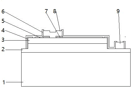
[0023] The preparation method of the GaN-based light-emitting diode chip of the present invention is suitable for the GaN-based light-emitting diode chip of the sapphire substrate that is installed, and the specific steps are as follows:

[0024] (1) First, coat 2- 6 μm (preferably 3 μm) thick positive photoresist, photolithography is carried out on the positive photoresist, and the pattern (the pattern of the desired mesa structure) that can be etched out of the mesa structure by subsequent ICP;

[0025] The photolithography process of the positive photoresist is completed through the steps of alignment, exposure, development, and drying: use a hot plate to bake at 98°C for 1 minute to 2 minutes for alignment, and then expose to ultraviolet light for 5 minutes. seconds to 20 seconds, and then developed with tetramethylammonium hydroxide for 10 seconds to 30 seconds after drying, and baked at 98°C for 1 to 2 minutes by using a hot plate.

[0026] (2) Utilize the ICP dry etchi...


PUM

PropertyMeasurementUnit
Thicknessaaaaaaaaaa
Thicknessaaaaaaaaaa

Abstract

The invention discloses a preparation method of a GaN-based light-emitting diode chip. The method comprises the following steps: (1) etching a table board structure from a p-type GaN layer to an n-type GaN layer of a GaN-based epitaxial wafer, preparing a table board on the n-type GaN layer, and simultaneously removing a residual photoresist on the surface; (2) growing current blocking layers on the outer surfaces of the p-type GaN layer and the n-type GaN layer; (3) etching the required patterns on the current blocking layers, reserving the current blocking layer on the upper surface of the p-type GaN layer and the current blocking layer on the side wall of a P/N junction; (4) depositing an nano-indium tin oxide (ITO) transparent conductive film on the surface of the p-type GaN layer; (5) respectively preparing a p-type electrode and an n-type electrode on the ITO transparent conductive film and the table board of the n-type GaN layer; and (6) preparing a passivation layer and exposing a metal electrode through photoetching. According to the method, the current blocking layers on the upper surface of the p-type GaN layer and the side wall of the P/N junction are reserved; the subsequent ITO transparent conductive film is prevented from contacting the metal electrode; the residual ITO or metal on the P/N junction is avoided; and electric leakage is not caused.

Description

technical field [0001] The invention relates to a method for preparing a GaN-based light-emitting diode chip, which belongs to the field of optoelectronic technology. Background technique [0002] Using sapphire (Sapphire, chemical formula Al 2 o 3 ) as the substrate, growing GaN semiconductors through organic chemical vapor deposition equipment has become the mainstream structure of blue LED components. [0003] Since the sapphire substrate is non-conductive, in the preparation of GaN-based LED chips, it is necessary to remove part of the material from the surface of the LED epitaxial wafer to the heavily doped n-type GaN layer, and place them on the p-type and n-type GaN materials respectively. Prepare p-type and n-type electrodes. [0004] The chemical bonding energy of GaN is high, and the high bonding energy and wide bandgap make the group III nitride materials chemically inert in nature, and are not corroded by chemical acid and alkali solutions at room temperature,...

Claims


Application Information

Patent Timeline
IPC IPC(8): H01L33/00H01L33/14
CPCH01L33/007H01L33/145
Inventor 彭璐杨肃伟黄博刘琦徐现刚
Owner SHANDONG INSPUR HUAGUANG OPTOELECTRONICS
Why Eureka
Try Eureka