
Bonding copper wire for fine-pitch IC packaging and manufacturing method thereof

A technology of bonding copper wire and fine pitch, which is applied in the field of bonding wire, can solve problems such as out-of-round deformed balls, short-circuited deformed balls, and increased hardness of copper wires, achieving high roundness, good symmetry, and product reliability high effect

Active Publication Date: 2015-12-16
NICHE TECH KAISER SHANTOU
View PDF14 Cites 0 Cited by
  • Summary
  • Abstract
  • Description
  • Claims
  • Application Information

AI Technical Summary

Problems solved by technology

[0003] Copper wire is different from gold wire and silver alloy wire. In the ball welding process, even if a FAB with high roundness is obtained, the deformed ball formed in the subsequent ball pressing process is more likely to be deformed than other wires (bonding wire). In some cases, it is easy to cause the edge of the deformed ball to exceed the range of the IC pad (Pad), and in a fine-pitch package (such as below 0.9mil), it is easy to cause two adjacent deformed balls to contact and short circuit
To overcome this problem, the Japanese NipponSteelMaterials patent (US20110011618A1) proposes to add doped phosphorus (P) to refine the grains, thereby increasing the roundness of the deformed ball. However, increasing the doped phosphorus will also increase the copper wire In addition, one of the inherent problems of copper wire itself is its high hardness, which will cause the non-dielectric layer under the IC pad to crack

Method used


Image

  • Bonding copper wire for fine-pitch IC packaging and manufacturing method thereof
  • Bonding copper wire for fine-pitch IC packaging and manufacturing method thereof
  • Bonding copper wire for fine-pitch IC packaging and manufacturing method thereof

Examples


Embodiment 1

[0027] The manufacturing method of the bonding copper wire used for fine-pitch IC packaging in this embodiment includes the following steps:

[0028] (1) Melting and casting: the copper with a purity of 4N and a main body oxygen content of 4ppm (weight) is subjected to vacuum smelting and directional continuous drawing process to obtain a wire rod with a diameter of 8 millimeters (mm);

[0029] (2) Wire drawing: the wire rod obtained in step (1) is drawn (the whole wire drawing process includes multiple wire drawing operations, and undergoes stages such as rough drawing, small drawing, fine drawing, and micro drawing) to obtain a wire with a diameter of 23 microns (um). Bonding copper wire;

[0030] During the wire drawing process, an intermediate annealing is carried out on the wire. The intermediate annealing is carried out when the wire drawing reaches a diameter of 0.0556 mm (mm). During the annealing process, N2 (nitrogen) is used as the annealing atmosphere. The effectiv...

Embodiment 2

[0034] The manufacturing method of the bonding copper wire used for fine-pitch IC packaging in this embodiment includes the following steps:

[0035] (1) Melting and casting: the copper with a purity of 4N and a main oxygen content of 3ppm (weight) is subjected to vacuum melting and directional continuous drawing process to obtain a wire rod with a diameter of 8 millimeters (mm);

[0036] (2) Wire drawing: the wire rod obtained in step (1) is drawn (the whole wire drawing process includes multiple wire drawing operations, and undergoes stages such as rough drawing, small drawing, fine drawing, and micro drawing) to obtain a wire with a diameter of 23 microns (um). Bonding copper wire;

[0037] During the wire drawing process, an intermediate annealing is carried out on the wire. The intermediate annealing is carried out when the wire is drawn to a diameter of 0.0384 mm (mm). During the annealing process, N2 (nitrogen) is used as the annealing atmosphere. The effective length o...

Embodiment 3

[0041] The manufacturing method of the bonding copper wire used for fine-pitch IC packaging in this embodiment includes the following steps:

[0042] (1) Melting and casting: the copper with a purity of 4N and a main oxygen content of 3ppm (weight) is subjected to vacuum melting and directional continuous drawing process to obtain a wire rod with a diameter of 8 millimeters (mm);

[0043] (2) Wire drawing: the wire rod obtained in step (1) is drawn (the whole wire drawing process includes multiple wire drawing operations, and undergoes stages such as rough drawing, small drawing, fine drawing, and micro drawing) to obtain a wire with a diameter of 23 microns (um). Bonding copper wire;

[0044] During the wire drawing process, an intermediate annealing is carried out on the wire. The intermediate annealing is carried out when the wire is drawn to a diameter of 0.0893 mm (mm). During the annealing process, N2 (nitrogen) is used as the annealing atmosphere. The effective length o...


PUM

PropertyMeasurementUnit
Diameteraaaaaaaaaa

Abstract

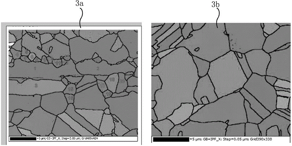
The invention provides a bonding copper wire for fine-pitch IC packaging. The bonding copper wire is made of copper with the purity being above 4N and the main body oxygen content being less than or equal to 5ppm (weight). The crystal size of the bonding copper wire is in normal distribution, and the average grain diameter of crystal is 1.6-1.8 micrometers. Preferably, the twin crystal density in the bonding copper wire is less than 35%. The invention further provides a manufacturing method of the bonding wire copper for fine-pitch IC packaging. The bonding wire copper provided by the invention is extremely low in hardness, the roundness of a deformation ball acquired in ball bonding is high, and the reliability is high, thereby being suitable for requirements of chip fine-pitch packaging.

Description

technical field [0001] The invention relates to a bonding wire for IC packaging, in particular to a bonding copper wire for fine-pitch IC packaging and a manufacturing method thereof. Background technique [0002] Bonding wire is used in the IC industry as the main connection method for connecting chips to external packaging substrates (substrates) and / or multilayer circuit boards (PCBs). When the transistor size in the chip is continuously reduced (now the most advanced logic chip, its minimum feature size is 14, 16nm), naturally the size of the pad on the chip will also shrink, and usually the diameter of the bonding wire is the pad 1 / 3 of the size, the diameter of the bonding wire burning ball FAB (freeairball, free air ball) is 1.8-2.0 times the diameter of the bonding wire, and the diameter of the deformed ball (SquashedFAB) is 2.5-2.8 times the diameter of the bonding wire. In order to meet the requirements of bonding and packaging of high-end chips with fine pitch, t...

Claims


Application Information

Patent Timeline
IPC IPC(8): H01L23/49H01L21/48C22F1/08
CPCH01L2224/45015H01L2224/45139H01L2224/45144H01L2224/45147H01L24/43H01L24/45H01L2924/00011H01L2924/20751H01L2924/20752H01L2924/00015H01L2924/01204H01L2924/01008H01L2924/01049
Inventor 周振基周博轩任智
Owner NICHE TECH KAISER SHANTOU
Learn More