

Preparation method of microarray chip and product thereof
A microarray chip and chip technology, applied in chemical instruments and methods, laboratory containers, laboratory utensils, etc., can solve the problems of no high-throughput three-dimensional micro-environment, cumbersome operation, high cost, etc., to facilitate analysis And the effect of research and operation is simple and fast
- Summary
- Abstract
- Description
- Claims
- Application Information
AI Technical Summary
Problems solved by technology
Method used
Image

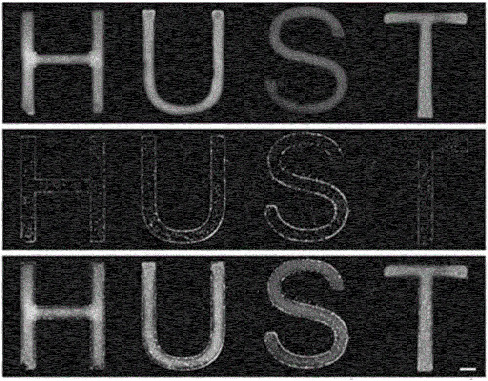
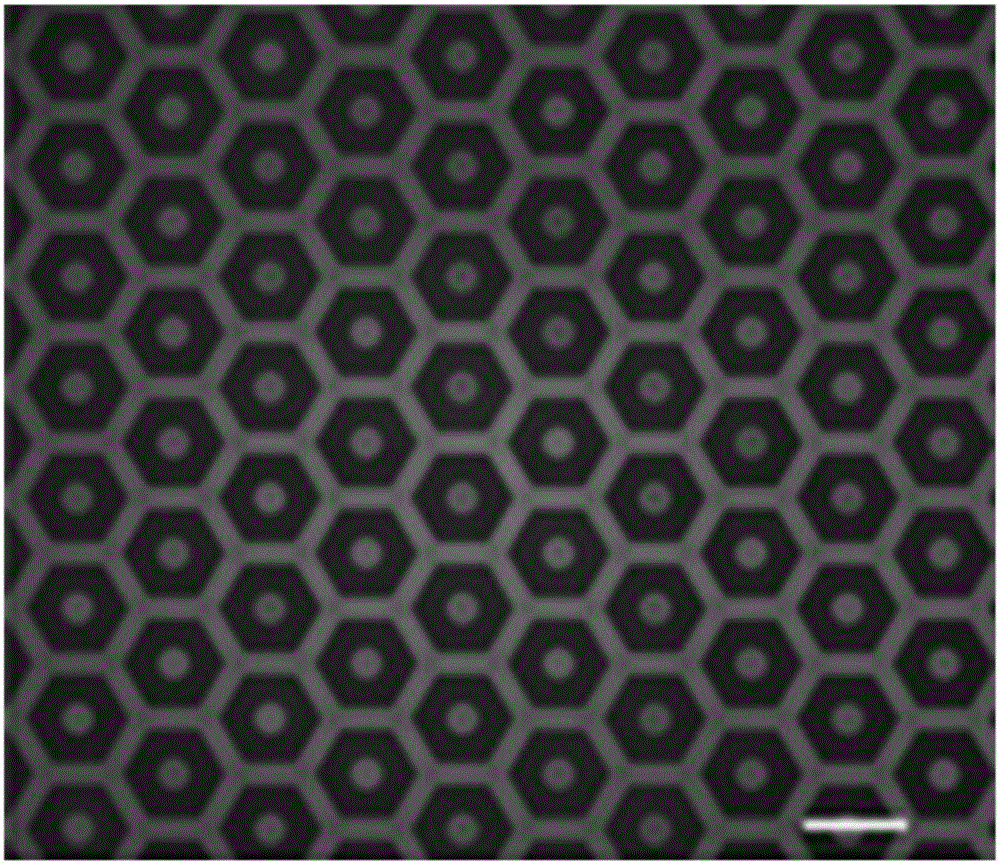
Examples
preparation example Construction
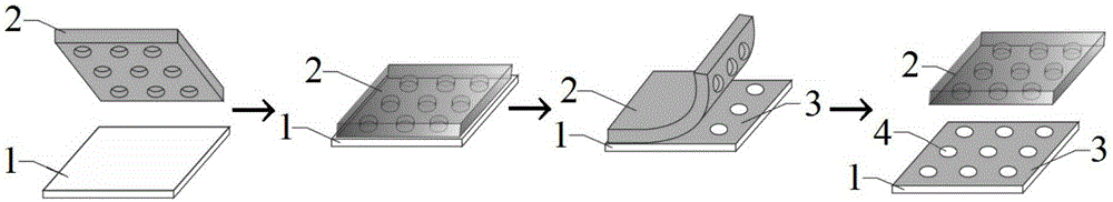
[0051] The preparation method of the basic chip is as follows:
[0052] (1) Design a photolithographic mask according to the morphology of the desired hydrophilic region and hydrophobic region; Similarly, when using a positive photoresist, such as SU-8, the shape of the mask is the same as that of the desired hydrophilic area;
[0053] (2) Utilize negative mold lithography or positive mold lithography to prepare a PDMS (polydimethylsiloxane) stamp with a corresponding shape, the PDMS stamp includes a raised portion and a depressed portion, and the raised portion The morphology of the depression corresponds to the hydrophobic region, and the morphology of the depression corresponds to the hydrophilic region;
[0054] (3) Treat the PDMS stamp and the substrate with plasma; wherein, the substrate surface is smooth and has a hydrophilic group; the hydrophilic group is a hydroxyl group, a carboxylic acid group, a sulfonic acid group, a phosphoric acid group, Amino groups, quatern...
Embodiment 1
[0072] The preparation of embodiment 1 glass substrate
[0073] Step 1: Make the positive mold by soft lithography technology
[0074] Throw the photoresist SU-8 (1070) on the cleaned and dried silicon wafer (700r18s, 2500r60s), and pre-baked to remove the solvent in the SU-8 glue (65°C 15min, 95°C 2hour), so that SU-8 The positive mold is better bonded to the silicon wafer, and then photolithography (3.5mJ / cm 2 ), the mask plate used in lithography is set according to the shape of the positive mold, and the photolithography time is 60s; then it is placed on a hot plate for post-baking (65°C 15min, 95°C 2hour), so that the positive mold and The silicon wafer is more closely bonded, and after being developed by a developer, the film is hardened (135°C) for more than 1 hour to achieve the effect of close adhesion between SU-8 and the silicon wafer, and the SU-8 anode with microstructure can be obtained. mold, and its height was measured to be about 20 μm.
[0075] Step 2: Pre...
Embodiment 2
[0081] Repeat Example 1 with the same steps described above, the difference is that in step 1, AZ-50 is used as the photoresist as AZ50, the mask plate is set according to the concave part of the PDMS stamp, and PDMS is prepared using the corresponding preparation process of AZ-50 seal.
PUM
| Property | Measurement | Unit |
|---|---|---|
| Diameter | aaaaa | aaaaa |
Abstract
Description
Claims
Application Information