Method for preparing plasma enhanced chemical vapor deposition (PECVD) silicon nitride protective film on surface of photoetching mask
A technology of silicon nitride protective film and photolithography mask, which is applied in the field of integrated circuits, can solve the problems of low process temperature, achieve the effects of low process temperature, prolong service life, and reduce damage
- Summary
- Abstract
- Description
- Claims
- Application Information
AI Technical Summary
Problems solved by technology
Method used
Image
Examples
Embodiment 1
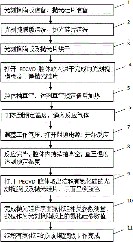
[0033] A method for preparing a PECVD deposited silicon nitride protective film on the surface of a photolithography mask, comprising the following process steps:
[0034] (1) Prepare the photolithography mask and polished silicon wafer to be produced;
[0035] (2) Clean the surface of the photolithographic mask and polished silicon wafer. The specific process of cleaning is: heat the photolithographic mask and polished silicon wafer to 80°C with a mass concentration of 92% sulfuric acid for 15 minutes, Rinse with deionized water for 20min, and use N 2 Blow dry and put it into a special quartz plate rack; dry the polished silicon wafer with a dryer for 7 minutes, and put it in a special flower basket for later use;
[0036] (3) Put the cleaned photolithography mask and polished silicon wafer into an oven and bake for 10 minutes at a baking temperature of 75°C;
[0037] (4) Put the baked photolithographic mask and clean polished silicon wafer into the PECVD cavity, requiring ...
Embodiment 2
[0046] A method for preparing a PECVD deposited silicon nitride protective film on the surface of a photolithography mask, comprising the following process steps:
[0047] (1) Prepare the photolithography mask and polished silicon wafer to be produced;
[0048] (2) Clean the surface of the photolithographic mask and polished silicon wafer. The specific cleaning process is: heat the photolithographic mask and polished silicon wafer to 90°C with a mass concentration of 90% sulfuric acid for 20 minutes. Rinse it with deionized water for 25min, and wash the photolithography mask with N 2 Blow dry and put it into a special quartz plate rack; dry the polished silicon wafer with a dryer for 8 minutes, and put it in a special flower basket for later use;
[0049] (3) Put the cleaned photolithography mask and polished silicon wafer into an oven and bake for 15 minutes at a baking temperature of 70°C;
[0050] (4) Put the baked photolithographic mask and clean polished silicon wafer i...
Embodiment 3
[0059] A method for preparing a PECVD deposited silicon nitride protective film on the surface of a photolithography mask, comprising the following process steps:
[0060] (1) Prepare the photolithography mask and polished silicon wafer to be produced;
[0061] (2) Clean the surface of the photolithographic mask and polished silicon wafer. The specific cleaning process is: heat the photolithographic mask and polished silicon wafer to 70°C with a mass concentration of 95% sulfuric acid for 10 minutes. Rinse with deionized water for 15 minutes, and then cover the photolithography mask with N 2 Blow dry and put it into a special quartz plate rack; dry the polished silicon wafer with a dryer for 6 minutes, and put it in a special flower basket for later use;
[0062] (3) Put the cleaned photolithography mask and polished silicon wafer into an oven and bake for 5 minutes at a baking temperature of 80°C;
[0063] (4) Put the baked photolithographic mask and clean polished silicon ...
PUM
| Property | Measurement | Unit |
|---|---|---|
| thickness | aaaaa | aaaaa |
| thickness | aaaaa | aaaaa |
| thickness | aaaaa | aaaaa |
Abstract
Description
Claims
Application Information
 - R&D Engineer
- R&D Manager
- IP Professional
- Industry Leading Data Capabilities
- Powerful AI technology
- Patent DNA Extraction
Browse by: Latest US Patents, China's latest patents, Technical Efficacy Thesaurus, Application Domain, Technology Topic, Popular Technical Reports.
© 2024 PatSnap. All rights reserved.Legal|Privacy policy|Modern Slavery Act Transparency Statement|Sitemap|About US| Contact US: help@patsnap.com


