LED structure and growth method thereof

A technology of LED structure and growth method, which is applied in the field of optoelectronics, can solve the problems such as the inability to reduce the stress of the well layer, and achieve the effects of increasing the rate of spontaneous emission and internal quantum efficiency, increasing the probability of overlapping, and reducing the degree of lattice mismatch

Inactive Publication Date: 2015-12-30
SHANDONG INSPUR HUAGUANG OPTOELECTRONICS
View PDF7 Cites 18 Cited by
  • Summary
  • Abstract
  • Description
  • Claims
  • Application Information

AI Technical Summary

Problems solved by technology

However, the material of the barrier layer in this patent is still GaN, and the doping ...

Method used


Image

  • LED structure and growth method thereof
  • LED structure and growth method thereof
  • LED structure and growth method thereof

Examples


Embodiment Construction

[0012] The technical scheme of the present invention is as follows:

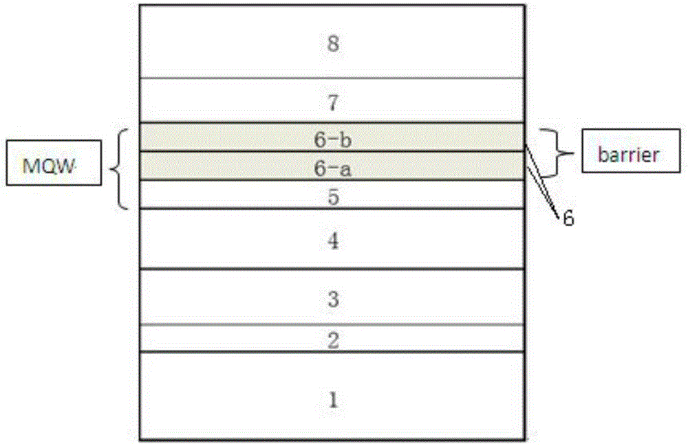
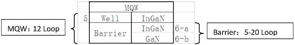
[0013] An LED structure, comprising a substrate layer, a GaN buffer layer, an undoped GaN layer, a Si-doped GaN layer, a P-type AlGaN layer and a P-type GaN layer; it is characterized in that the Si-doped GaN layer and P-type AlGaN layers include multiple quantum well active regions of InGaN / GaN superlattice barrier layers.

[0014] Preferably, according to the present invention, the InGaN / GaN superlattice barrier layer includes InGaN barrier layers and GaN barrier layers that are grown alternately and periodically.

[0015] According to the present invention, preferably, the multiple quantum well active region includes InGaN well layers and InGaN / GaN superlattice barrier layers that are grown alternately and periodically.

[0016] According to the present invention, preferably, the alternating period of the InGaN barrier layer and the GaN barrier layer in the InGaN / GaN superlattice barrier layer is 5-20 times.

[00...


PUM

PropertyMeasurementUnit
Thicknessaaaaaaaaaa

Abstract

The invention relates to an LED structure. The LED structure comprises a substrate layer, a GaN buffer layer, a non-doped GaN layer, a Si-doped GaN layer, a P-type AlGaN layer and a P-type GaN layer. The LED structure is characterized in that a multi-quantum well active region containing InGaN/GaN superlattice barrier layers is located between the Si-doped GaN layer and the P-type AlGaN layer. According to the LED structure of the invention, the InGaN/GaN superlattice barrier layers are adopted to replace traditional GaN barrier layers, and therefore, lattice mismatch between barrier layers and potential well layers can be decreased, and the crystal quality of the MQW can be can effectively changed, and the overlap probability of electron-hole wave function can be improved, and the spontaneous emission rate and internal quantum efficiency of the multi-quantum well can be improved, and finally, the luminous efficiency of a GaN-based LED device can be improved.

Description

Technical field [0001] The invention relates to an LED structure and a growth method thereof, and belongs to the technical field of optoelectronics. Background technique [0002] GaN-based III-V group nitride is an important wide-bandgap semiconductor material with direct band gap. Group III nitrides represented by GaN, InN, and AlN are direct bandgap semiconductor materials with excellent photoelectric properties and are indispensable materials in the manufacture of short-wavelength light-emitting diodes (LEDs) and photodetectors. The band gap of GaN is 3.4 electron volts (eV), and the band gap of InN is 0.7 eV. The corresponding emission wavelengths of these two materials are located in the ultraviolet and infrared regions, respectively. [0003] GaN-based materials have excellent mechanical and chemical properties, and excellent photoelectric properties. The band gap ranges from 0.7eV (IN) to 6.2 (AlN) at room temperature. The emission wavelengths cover far infrared, infrared, ...

Claims


Application Information

Patent Timeline
IPC IPC(8): H01L33/06H01L33/00
CPCH01L33/06H01L33/007
Inventor 李毓锋曲爽逯遥王成新徐现刚
Owner SHANDONG INSPUR HUAGUANG OPTOELECTRONICS
Why Eureka
Try Eureka