

Textured structure of crystalline silicon solar cell and preparation method thereof
A technology of solar cells and crystalline silicon, which is applied in the field of solar cells and can solve problems such as unfavorable industrial production and complicated processes
- Summary
- Abstract
- Description
- Claims
- Application Information
AI Technical Summary
Problems solved by technology
Method used
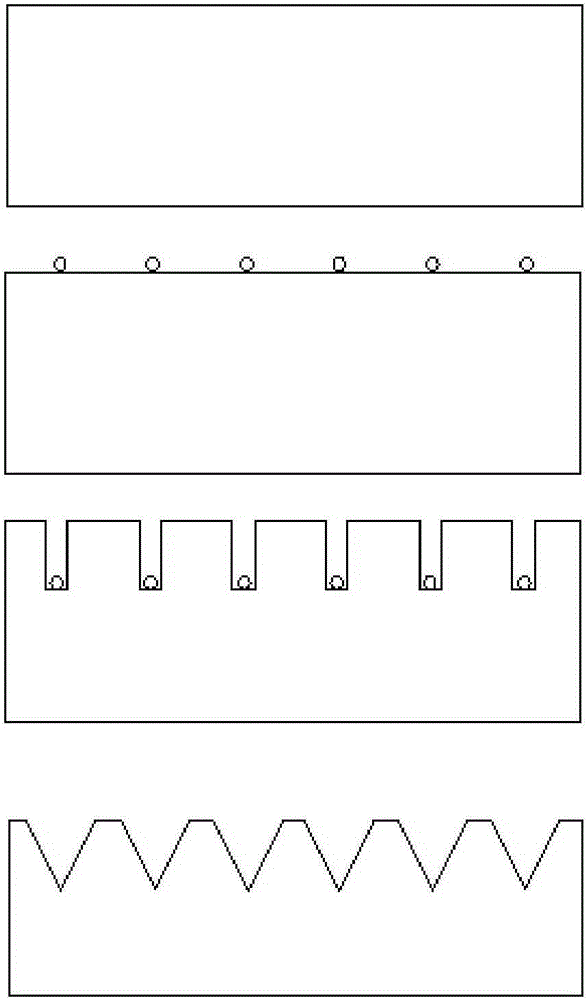
Image

Examples
Embodiment 1
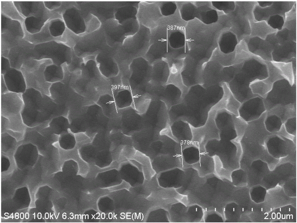
[0092] see image 3 Shown, a kind of preparation method of the textured structure of polycrystalline silicon solar cell is made up of following steps:
[0093] (1) cleaning the silicon wafer and removing the surface damage layer;
[0094] (2) Putting the above-mentioned silicon chip into a chemical etching solution containing metal ions to form a nanowire or porous silicon structure on the surface of the silicon chip; the temperature is 30° C., and the time is 2 minutes;
[0095] The metal ion is selected from silver ion;
[0096] The chemical etching solution is selected from HF and H 2 o 2 mixed solution;
[0097] Among them, the concentration of HF is 10mol / L, H 2 o 2 The concentration is 0.4mol / L;
[0098] (3) Putting the above-mentioned silicon chip into the first chemical etching solution for corrective etching, so that the above-mentioned nanowire or porous silicon structure forms a nano-deep hole structure;
[0099] The first chemical etching solution is HNO 3...
Embodiment 2
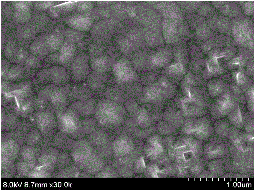
[0111] see Figure 4 Shown, a kind of preparation method of the textured structure of polycrystalline silicon solar cell is made up of following steps:
[0112] (1) cleaning the silicon wafer and removing the surface damage layer;
[0113] (2) Putting the above-mentioned silicon chip into a chemical etching solution containing metal ions to form a nanowire or porous silicon structure on the surface of the silicon chip; the temperature is 30° C., and the time is 2 minutes;
[0114] The metal ion is selected from silver ion;
[0115] The chemical etching solution is selected from HF and H 2 o 2 mixed solution;
[0116] Among them, the concentration of HF is 10mol / L, H 2 o 2 The concentration is 0.4mol / L;
[0117] (3) Putting the above-mentioned silicon chip into the first chemical etching solution for corrective etching, so that the above-mentioned nanowire or porous silicon structure forms a nano-deep hole structure;
[0118] The first chemical etching solution is HNO ...
PUM
| Property | Measurement | Unit |
|---|---|---|
| size | aaaaa | aaaaa |
| size | aaaaa | aaaaa |
| depth | aaaaa | aaaaa |
Abstract
Description
Claims
Application Information