
Manufacturing method for hybrid heterojunction solar cell

A solar cell and heterojunction technology, applied in circuits, photovoltaic power generation, electrical components, etc., can solve the problems of low photoelectric conversion efficiency, narrow spectral response range, and low utilization rate of sunlight of solar cells, and achieve environmentally friendly use, The principle is scientific and reasonable, and the effect of improving the photoelectric conversion performance

Inactive Publication Date: 2016-01-13
QINGDAO UNIV
View PDF6 Cites 9 Cited by
  • Summary
  • Abstract
  • Description
  • Claims
  • Application Information

AI Technical Summary

Problems solved by technology

However, due to TiO 2 The band gap is relatively large, and the above patents all have the disadvantages of narrow spectral response range and low utilization rate of sunlight, which leads to low photoelectric conversion efficiency of solar cells
So far, no one has reported that it can improve TiO 2 The interface contact effect of nanorod array heterojunction solar cells can also broaden the research work of its light absorption range

Method used


Image

  • Manufacturing method for hybrid heterojunction solar cell
  • Manufacturing method for hybrid heterojunction solar cell
  • Manufacturing method for hybrid heterojunction solar cell

Examples


Embodiment 1

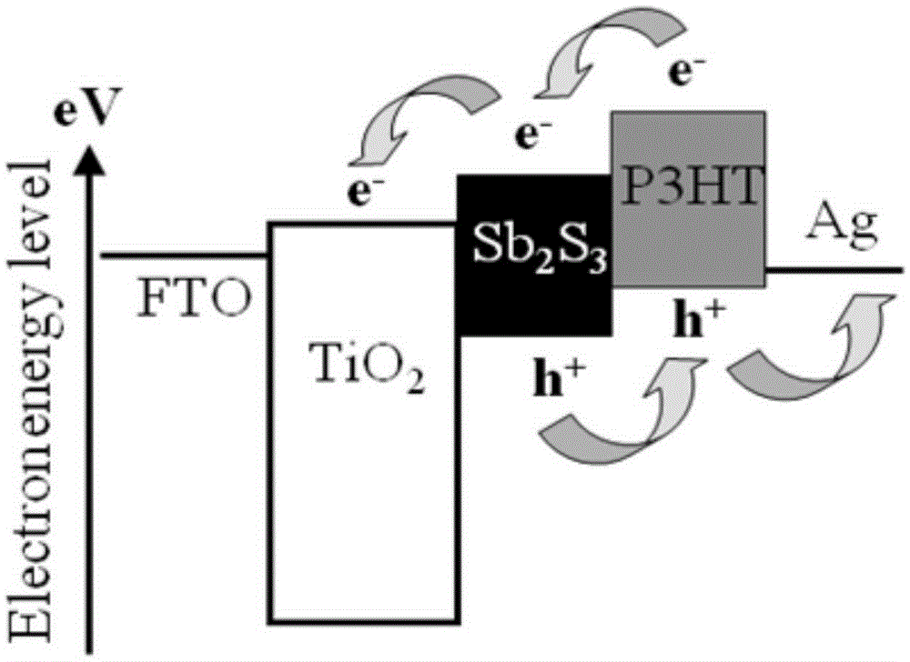
[0024] The preparation method of the hybrid heterojunction solar cell involved in this example includes preparing a conductive glass substrate, preparing an ordered TiO 2 Nanorod array film layer, preparation of antimony trisulfide (Sb 2 S 3 ) nano film layer, prepare 3-hexylthiophene (P3HT) nano film layer and prepare silver (Ag) film electrode five steps:

[0025] (1) Preparation of conductive glass substrate: Cut the FTO transparent conductive glass with a thickness of 0.8mm into a square with a size of 1cm×1cm, ultrasonically clean it with acetone, ethanol and deionized water in turn, and dry it with nitrogen to complete the conductive glass substrate preparation of

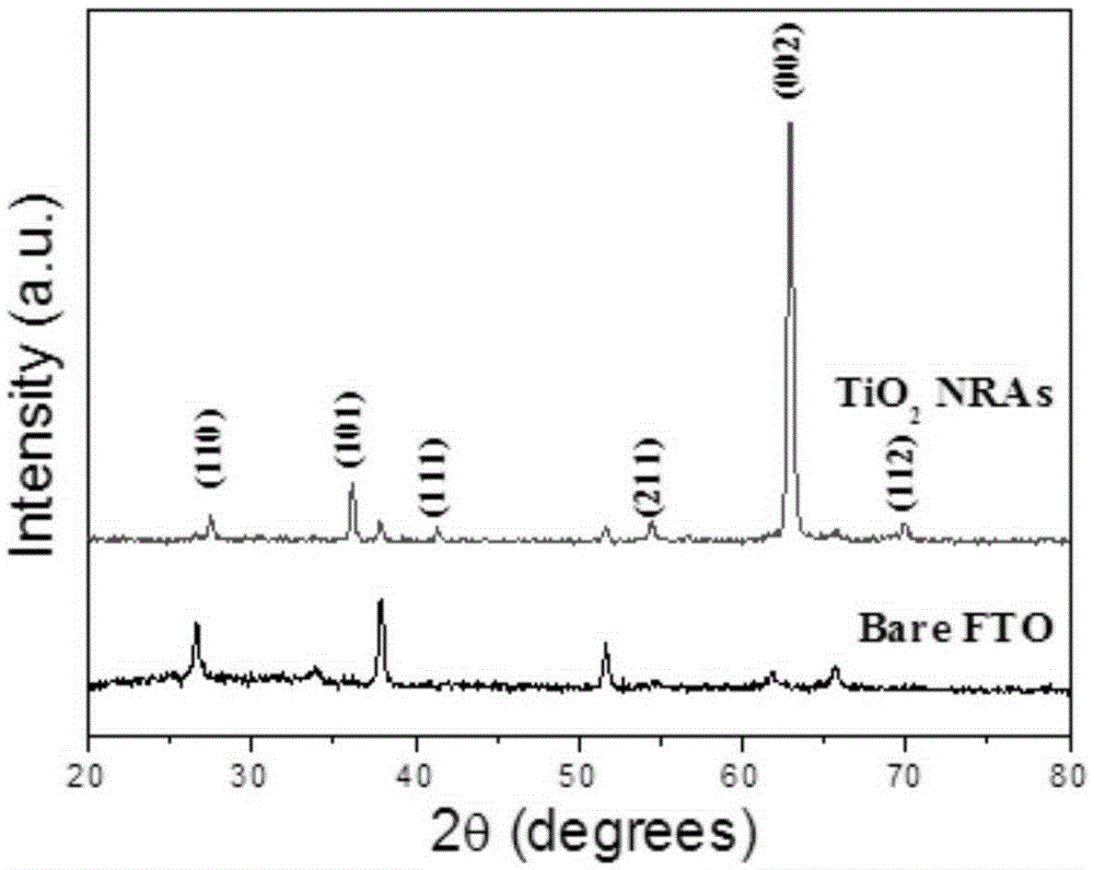
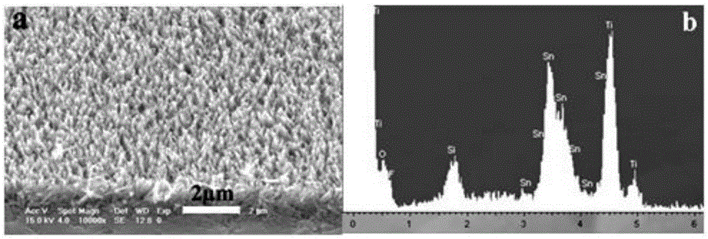
[0026] (2) Preparation of ordered TiO 2 Nanorod array film layer: Mix 0.2ml of TTIP, 10ml of 37% hydrochloric acid (HCl) aqueous solution and 20ml of deionized water under magnetic stirring to obtain 30ml of TiO 2 precursor solution, the conductive glass substrate and TiO 2 The precursor solution was pla...

Embodiment 2

[0034] The process steps of this embodiment are the same as those of Example 1, except that the thickness of the FTO transparent conductive glass in step (1) is 2 mm, and the size cut into a square of 4 × 4 cm, the prepared ordered TiO 2 The nanorod array film layer is uniformly and orderly distributed, with a high density, a diameter of 75-90nm, and a length of 0.8-1.1μm

Embodiment 3

[0036] The process step of this embodiment is the same as that of Example 1, except that the volume of TTIP in step (2) is 0.4ml, and the volume of hydrochloric acid (HCl) aqueous solution of 37% by mass is 15ml, and the prepared ordered TiO 2 The film layer of the nanorod array is evenly and orderly distributed, the density is small, the diameter is 80-95nm, and the length is 0.9-1.2μm.


PUM

PropertyMeasurementUnit
diameteraaaaaaaaaa
lengthaaaaaaaaaa
diameteraaaaaaaaaa

Abstract

The invention belongs to the technical field of solar cell manufacturing, and relates to a manufacturing method for a hybrid heterojunction solar cell. The manufacturing method comprises the five steps of manufacturing a conductive glass substrate, manufacturing an ordered TiO2 nanorod array film layer, manufacturing an Sb2S3 nano film layer, manufacturing a P3HT nano film layer and manufacturing an Ag film electrode. The ordered TiO2 nanorod array film layer is manufactured by adopting a one-step low-temperature hydrothermal method, the Sb2S3 nano film layer is formed by depositing Sb2S3 on the surface of the ordered TiO2 nanorod array film layer by adopting a chemical liquid phase deposition method, the P3HT nano film layer is formed by depositing P3HT on the surface of the Sb2S3 nano film layer by adopting a spin-coating method, and an Ag electrode is plated on the surface of the P3HT nano film layer by adopting a thermal evaporation method or a magnetron sputtering method at last, thereby manufacturing the TiO2 / Sb2S3 / P3HT hybrid heterojunction solar cell. The manufacturing method has the advantages of simple and controllable process, scientific and reasonable principle, low energy consumption and production cost, high operability, energy conservation, environment protection and friendly operating environment, can be recycled and reused, and is suitable for large-scale production, popularization and use.

Description

Technical field: [0001] The invention belongs to the technical field of solar cell preparation, and relates to a method for preparing a hybrid heterojunction solar cell. 2 ) The light absorption range and photogenerated carrier mobility of the nanorod array, reduce the recombination rate of photogenerated carriers, and enhance the photoelectric conversion performance of hybrid heterojunction solar cells. Background technique: [0002] With the rapid development of the world economy, fossil energy such as coal, oil and natural gas has been consumed in large quantities, and at the same time it has caused serious environmental pollution problems. Sustained development is of great strategic significance. Solar energy is green, renewable and inexhaustible, and it is the energy source with the most potential to replace fossil fuels. Solar cells, also known as solar chips and photocells, are devices that directly convert light energy into electrical energy through the photoelectr...

Claims


Application Information

Patent Timeline
Patent Type & Authority Applications(China)
IPC IPC(8): H01L51/48H01L51/46H01L51/44B82Y30/00
CPCB82Y30/00H10K30/00H10K30/352H10K30/35H10K30/80Y02E10/549Y02P70/50
Inventor 王凤云张洪超商蕾韩振莲
Owner QINGDAO UNIV
Learn More