AlGaN/GaN high electron mobility transistor with multi-channel fin-type structure

A technology with high electron mobility and fin structure, applied in the field of microelectronics, can solve the problems of poor gate control capability and low current drive capability of FinFET structure devices, and achieve enhanced gate control capability, device gain capability, and good switching characteristics Effect

Inactive Publication Date: 2016-01-27
XIDIAN UNIV
View PDF3 Cites 13 Cited by
  • Summary
  • Abstract
  • Description
  • Claims
  • Application Information

AI Technical Summary

Problems solved by technology

[0009] The purpose of the present invention is to provide a AlGaN / GaN high electron mobility transistor with a multi-channel fin structure to solve the above problems of poor gate control capability of multi-channel heterojunction devices and low current drive capability of FinFET structure devices. Meet the application requirements of GaN-based electronic devices in the fields of high-voltage switches and digital circuits

Method used


Image

  • AlGaN/GaN high electron mobility transistor with multi-channel fin-type structure
  • AlGaN/GaN high electron mobility transistor with multi-channel fin-type structure
  • AlGaN/GaN high electron mobility transistor with multi-channel fin-type structure

Examples


Embodiment 1

[0035] Embodiment 1: Fabricate a dual-channel fin-type AlGaN / GaN high electron mobility transistor with a gate fin width of 100 nm.

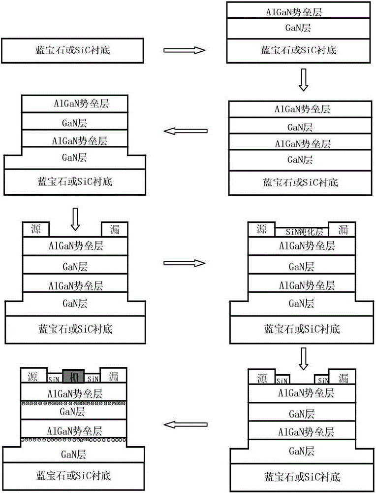
[0036] Step 1. Using the MOCVD process, epitaxially grow the double heterojunction.

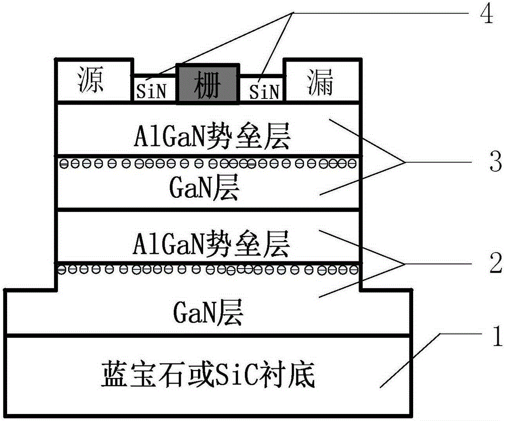
[0037] 1.1) On the SiC substrate, grow an intrinsic GaN layer with a thickness of 1 μm;

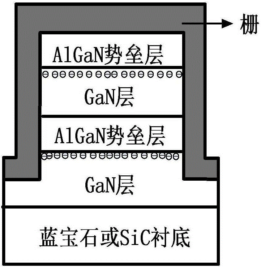
[0038] 1.2) A 15nm-thick AlGaN barrier layer is grown on the intrinsic GaN layer, wherein the Al composition is 35%, and a two-dimensional electron gas is formed at the contact position between the intrinsic GaN layer and the AlGaN barrier layer, and the first layer of AlGaN / GaN heterojunction;

[0039] 1.3) regrowing a second intrinsic GaN layer with a thickness of 20 nm on the 15 nm thick AlGaN barrier layer;

[0040] 1.4) A second 15nm-thick AlGaN barrier layer is grown on the second intrinsic GaN layer, wherein the Al composition is 35%, to obtain a second layer of AlGaN / GaN heterojunction.

[0041] The process condition of this step is: with NH 3 is the N source,...

Embodiment 2

[0063] Embodiment 2: Fabricate a three-channel fin-type AlGaN / GaN high electron mobility transistor with a gate fin width of 50 nm.

[0064] Step 1. Using the MOCVD process, epitaxially grow the triple heterojunction.

[0065] 1a) On a sapphire substrate, with NH 3 N source, MO source is Ga source, the growth temperature is 1000°C, and the intrinsic GaN layer with a thickness of 1.5 μm is grown;

[0066] 1b) On the intrinsic GaN layer, grow a 20nm-thick AlGaN barrier layer, in which the Al composition is 30%, and form a two-dimensional electron gas at the contact position between the intrinsic GaN layer and the AlGaN barrier layer, and obtain the first layer of AlGaN / GaN heterojunction;

[0067] 1c) growing a second intrinsic GaN layer with a thickness of 25 nm on the first AlGaN barrier layer with a thickness of 20 nm;

[0068] 1d) growing a second 20nm-thick AlGaN barrier layer on the second intrinsic GaN layer, wherein the Al composition is 30%, to obtain a second layer...

Embodiment 3

[0091] Embodiment 3: Fabricate a dual-channel fin-type AlGaN / GaN high electron mobility transistor with a gate fin width of 30 nm.

[0092] Step A. Using the MOCVD process, epitaxially grow the double heterojunction.

[0093] in NH 3 is the N source, the MO source is the Ga source, and the growth temperature is 1000°C, first grow an intrinsic GaN layer with a thickness of 2 μm on the SiC substrate; then grow a 25nm thick GaN layer on the intrinsic GaN layer. The AlGaN barrier layer, in which the Al composition is 25%, forms a two-dimensional electron gas at the contact position between the intrinsic GaN layer and the AlGaN barrier layer, and obtains the first layer of AlGaN / GaN heterojunction; then the 25nm thick AlGaN barrier layer A second intrinsic GaN layer with a thickness of 30nm is grown on the barrier layer; finally, a second AlGaN barrier layer with a thickness of 25nm is grown on the second intrinsic GaN layer, wherein the Al composition is 25%, and the second layer...


PUM


Abstract

The invention discloses a AlGaN / GaN high electron mobility transistor structure with a multi-channel fin-type structure and a manufacturing method, wherein the AlGaN / GaN high electron mobility transistor is designed mainly to solve the problems of the poor gate control ability of a multi-channel apparatus and low electric current of a FinFET apparatus; the AlGaN / GaN high electron mobility transistor comprises a substrate (1), a first layer AlGaN / GaN heterojunction (2), a SiN passivation layer (4) and a source electrode, a drain electroce, and a gate electrode successively from bottom to top; the source electrode and the drain electrode are located on AlGaN potential barrier layers on top layers at two sides of the SiN passivation layer respectively; the AlGaN / GaN high electron mobility transistor is characterized in that a GaN layer and the AlGaN potential barrier layer are set between the first layer AlGaN / GaN heterojunction and the SiN passivation layer so as to form a second layer AlGaN / GaN heterojuntion (3); and the gate electrode covers the top portion of a second layer heterojuntion and the two side walls of the first and the second heterojunctions. According to the invention, the gate control ability is strong; the saturation current is large; the subthreshold property is good; and the AlGaN / GaN high electron mobility transistor can be used for microwave power apparatus with a shrot gate length, low power consumption and low noise.

Description

technical field [0001] The invention belongs to the technical field of microelectronics, and relates to the structure and manufacture of semiconductor devices, in particular to an AlGaN / GaN high electron mobility transistor HEMT with a multi-channel fin structure, which can be used to manufacture large-scale integrated circuits. Background technique [0002] In recent years, the third-generation wide-bandgap semiconductors represented by SiC and GaN have the characteristics of large bandgap, high breakdown electric field, high thermal conductivity, high saturation electron velocity, and high concentration of two-dimensional electron gas 2DEG at the heterojunction interface. make it receive widespread attention. In theory, high electron mobility transistor HEMT, light emitting diode LED, laser diode LD and other devices made of these materials have obvious superior characteristics than existing devices, so in recent years, researchers at home and abroad have conducted extensi...

Claims


Application Information

Patent Timeline
Patent Type & Authority Applications(China)
IPC IPC(8): H01L29/778H01L21/335
CPCH01L29/7783H01L29/66462
Inventor 王冲魏晓晓郝跃何云龙郑雪峰马晓华张进成
Owner XIDIAN UNIV
Why Eureka
Try Eureka