

Film resistor and preparation method thereof
A technology of thin film resistors and resistive layers, which is applied in thin film resistors, resistors, resistor manufacturing, etc., and can solve problems such as thin film resistor failure and general moisture resistance of the protective layer
- Summary
- Abstract
- Description
- Claims
- Application Information
AI Technical Summary
Problems solved by technology
Method used
Image

Examples
preparation example Construction
[0044] The preparation method of above-mentioned film resistor, comprises the following steps:
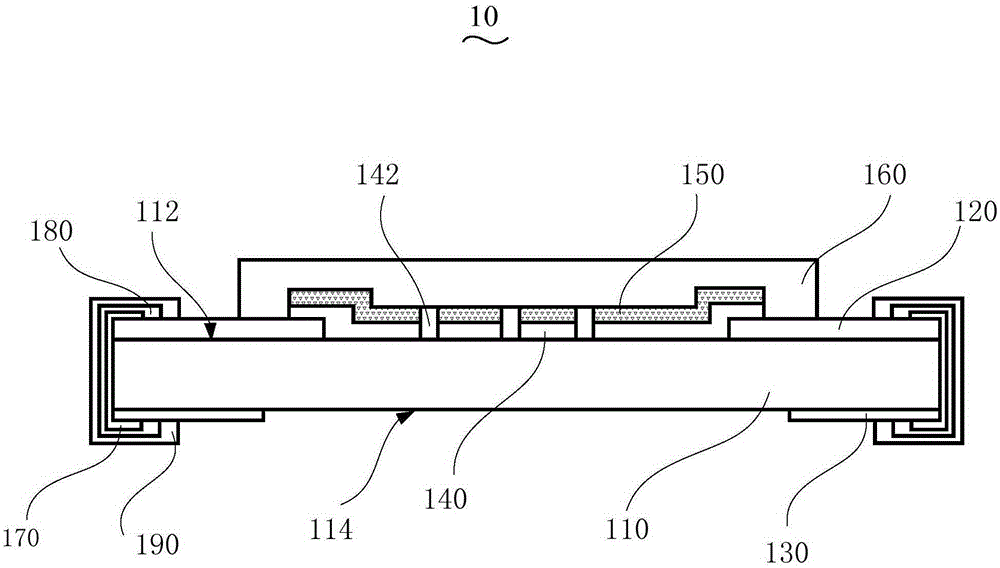
[0045] Step S1 , preparing two surface electrodes 120 spaced apart from each other on the surface 112 of the insulating substrate 110 .
[0046] The insulating substrate 110 is a ceramic insulating substrate or a glass insulating substrate. Preferably, the insulating substrate 110 is an aluminum oxide ceramic substrate with a purity of 96 wt % to 99.9 wt %, more preferably an aluminum oxide ceramic substrate with a purity of 99 wt % to 99.9 wt %.
[0047] It should be noted that, according to the performance requirements of the insulating substrate 110 , the insulating substrate 110 can also be modified, and a modified layer is deposited on the surface of the insulating substrate 110 to improve the flatness of the insulating substrate 110 surface. The material of the modified layer is silicide, which is formed by thin film deposition techniques such as thermal evaporation depositi...
Embodiment 1
[0085] Fabricate thin film resistors as follows:
[0086] (1) Two surface electrodes 120 are formed on the surface 112 of the insulating substrate 110 by screen printing, and two back electrodes 130 are formed on the back surface 114 of the insulating substrate 110 by screen printing.
[0087] The insulating substrate 110 is a ceramic insulating substrate, and the purity (mass percentage) of the substrate is 99-99.9% Al 2 o 3 Ceramic substrate.
[0088] The surface electrode 120 is made of silver and silver-palladium alloy, and the palladium content (accounting for the mass percentage of the conductive electrode paste) is 20%.
[0089] The material of the back electrode 130 is silver and silver-palladium alloy, and the palladium content (accounting for the mass percentage of the conductive electrode paste) is 0.5%.
[0090] (2) Forming the resistance layer 140 on the surfaces of the surface electrodes 120 and the insulating substrate 110 .
[0091] The material of the resi...
Embodiment 2
[0105] Fabricate thin film resistors as follows:
[0106] (1) Two surface electrodes 120 are formed by screen printing on the surface 112 of the insulating substrate 110 , and a back electrode 130 is formed on the back surface 114 of the insulating substrate 110 by screen printing.
[0107] The insulating substrate 110 is a ceramic insulating substrate, and the purity (mass percentage) of the substrate is 96-99.9% Al 2 o 3 Ceramic substrate.
[0108] The surface electrode 120 is made of silver and silver-palladium alloy, and the palladium content (accounting for the mass percentage of the conductive electrode paste) is 30%.
[0109] The material of the back electrode 130 is silver and silver-palladium alloy, and the palladium content (accounting for the mass percentage of the conductive electrode paste) is 0.75%.
[0110] (2) Forming the resistance layer 140 on the surfaces of the surface electrodes 120 and the insulating substrate 110 .
[0111] The material of the resist...
PUM
| Property | Measurement | Unit |
|---|---|---|
| Thickness | aaaaa | aaaaa |
| Thickness | aaaaa | aaaaa |
| Thickness | aaaaa | aaaaa |
Abstract
Description
Claims
Application Information