
Method for preparing base-region graded doped silicon carbide thin film epitaxy layer

A silicon carbide and silicon carbide substrate technology, applied in gaseous chemical plating, metal material coating process, superimposed layer plating and other directions, can solve problems affecting device performance, high bond strength of silicon carbide, lattice damage, etc. , to simplify the preparation process, improve device performance, and achieve the effect of complete lattice

Inactive Publication Date: 2016-03-02
GLOBAL ENERGY INTERCONNECTION RES INST CO LTD +2
View PDF3 Cites 4 Cited by
  • Summary
  • Abstract
  • Description
  • Claims
  • Application Information

AI Technical Summary

Problems solved by technology

However, due to the high bond strength of silicon carbide, the doping in the device manufacturing process cannot use the diffusion process, and can only be controlled by epitaxy and high-temperature ion implantation.
High-temperature ion implantation will cause a lot of lattice damage and form a large number of lattice defects, which are difficult to completely eliminate even with annealing, seriously affecting the performance of the device, and the efficiency of ion implantation is very low, so it is not suitable for large-area doping

Method used


Image

  • Method for preparing base-region graded doped silicon carbide thin film epitaxy layer

Examples


Embodiment 1

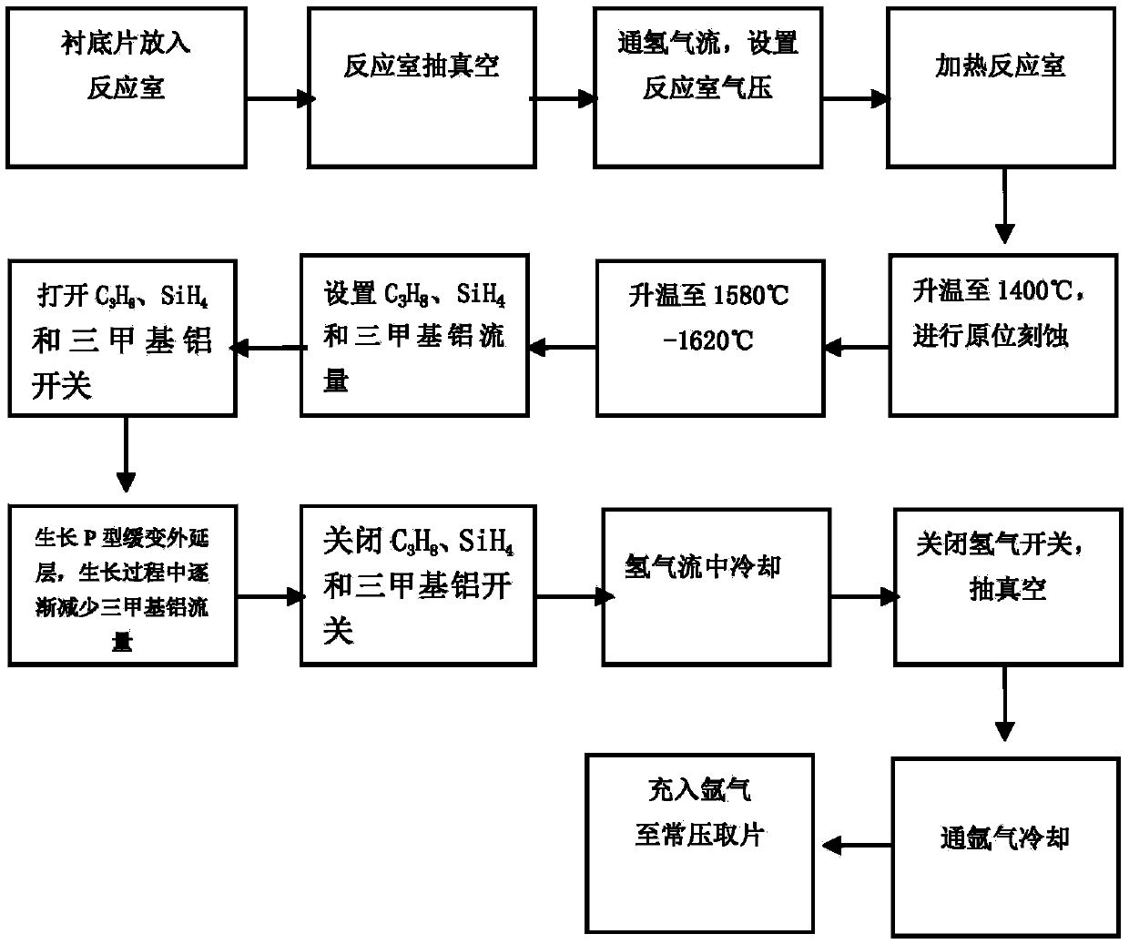
[0043] In step 1, the silicon carbide substrate is placed in the reaction chamber of the silicon carbide CVD equipment.

[0044] (1.1) Selection bias Crystal orientation 4° (bias The crystal orientation 4° refers to the 4H silicon carbide substrate with a deviation of 4° in the 11-20 direction in the 0001 direction, and is placed in the reaction chamber of the silicon carbide CVD equipment;

[0045] (1.2) Evacuate the reaction chamber until the pressure of the reaction chamber is lower than 1×10 -7 mbar.

[0046] In the second step, the reaction chamber is heated in a hydrogen stream.

[0047] (2.1) Open the hydrogen switch leading to the reaction chamber, and control the hydrogen flow to gradually increase to 60L / min;

[0048] (2.2) Turn on the vacuum pump to extract the gas in the reaction chamber, and keep the pressure of the reaction chamber at 100mbar;

[0049] (2.3) Gradually increase the power of the heating source to slowly increase the temperature of the reacti...

Embodiment 2

[0066] In step 1, the silicon carbide substrate is placed in the reaction chamber of the silicon carbide CVD equipment.

[0067] (1.1) Selection bias Crystal orientation 8° (bias The crystal orientation of 8° refers to the 4H silicon carbide substrate that deviates from the 11-20 direction by 8° in the 0001 direction, and is placed in the reaction chamber of the silicon carbide CVD equipment;

[0068] (1.2) Evacuate the reaction chamber until the pressure of the reaction chamber is lower than 1×10 -7 mbar.

[0069] In the second step, the reaction chamber is heated in a hydrogen stream.

[0070] (2.1) Open the hydrogen switch leading to the reaction chamber, and control the hydrogen flow to gradually increase to 60L / min;

[0071] (2.2) Turn on the vacuum pump to extract the gas in the reaction chamber, and keep the pressure of the reaction chamber at 100mbar;

[0072] (2.3) Gradually increase the power of the heating source to slowly increase the temperature of the reac...


PUM


Abstract

The invention relates to a method for preparing a base-region graded doped silicon carbide thin film epitaxy layer. The method comprises the steps that 1, a silicon carbide substrate is placed in a reaction chamber of silicon carbide CVD equipment, and the reaction chamber is vacuated; 2, H2 is introduced into the reaction chamber till the air pressure of the reaction chamber reaches 100 mbar, the air pressure of the reaction chamber is kept constant, the flow of H2 is gradually increased to 60 L / min, and gas continues to be introduced into the reaction chamber; 3, a high-frequency coil induction heater RF is started, the power of the heater is gradually increased, and when the temperature of the reaction chamber gradually rises to 1,400 DEG C, in-situ etching is carried out; and 4, when the temperature of the reaction chamber reaches 1,580 DEG C to 1,600 DEG C, the temperature and pressure are kept constant, the flow of an Al source is set, C3H8 and SiH4 are introduced into the reaction chamber, and the P-type graded doped silicon carbide thin film epitaxy layer is slowly grown by gradually adjusting the flow of the Al source introduced into the reaction chamber. According to the method, the CVD equipment of silicon carbide is utilized, the silicon carbide epitaxy layer with the controllable longitudinal doping concentration gradient is prepared, and the requirement for preparation of the gradient low-doped epitaxy layer is met.

Description

technical field [0001] The invention relates to the technical field of semiconductor device manufacturing, in particular to an epitaxy preparation method of a base region graded doped silicon carbide thin film. Background technique [0002] Silicon carbide has the advantages of wide band gap, high thermal conductivity, high breakdown strength, high electron saturation drift speed, high hardness, etc., and also has strong chemical stability. These excellent physical and electrical properties make silicon carbide have many advantages in applications. The band gap enables the intrinsic carrier of silicon carbide to maintain a low concentration at high temperature, so it can work at very high temperature. The high breakdown field strength allows silicon carbide to withstand high electric field strengths, which makes silicon carbide useful for making high-voltage, high-power semiconductor devices. High thermal conductivity makes silicon carbide have good heat dissipation, which...

Claims


Application Information

Patent Timeline
Patent Type & Authority Applications(China)
IPC IPC(8): C23C16/32C23C16/44
CPCC23C16/325C23C16/44C23C28/048
Inventor 钮应喜杨霏温家良陈新
Owner GLOBAL ENERGY INTERCONNECTION RES INST CO LTD
Learn More