Semiconductor device and manufacturing method thereof, and electronic apparatus

A manufacturing method and semiconductor technology, applied in semiconductor devices, semiconductor/solid-state device manufacturing, circuits, etc., can solve the problems that affect the normal progress of the IGBT backside process, and the Taiko wafer is prone to breakage, etc., and achieves low cost, good uniformity, The effect of mature and simple process

Active Publication Date: 2016-03-02
SEMICON MFG INT (SHANGHAI) CORP
View PDF3 Cites 6 Cited by
  • Summary
  • Abstract
  • Description
  • Claims
  • Application Information

AI Technical Summary

Problems solved by technology

[0004] figure 1 It shows an existing IGBT manufacturing process, in which Taiko grinding is mostly used for IGBT wafer thinning (thickness is 50-60 μ

Method used


Image

  • Semiconductor device and manufacturing method thereof, and electronic apparatus
  • Semiconductor device and manufacturing method thereof, and electronic apparatus
  • Semiconductor device and manufacturing method thereof, and electronic apparatus

Examples


Embodiment 1

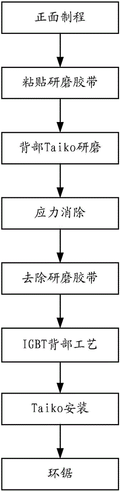
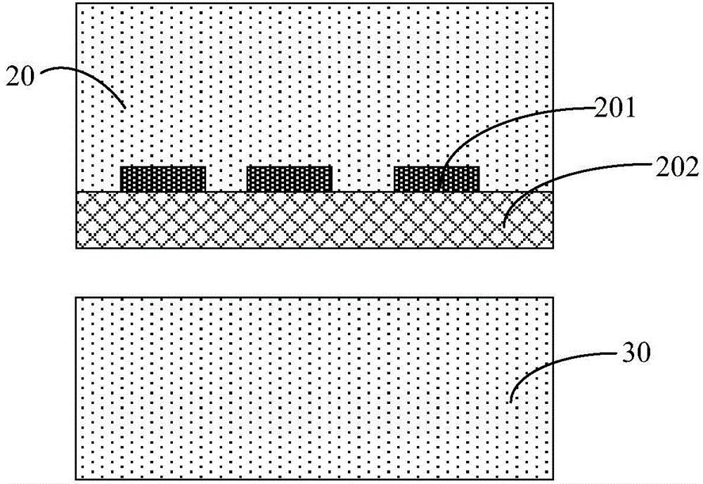
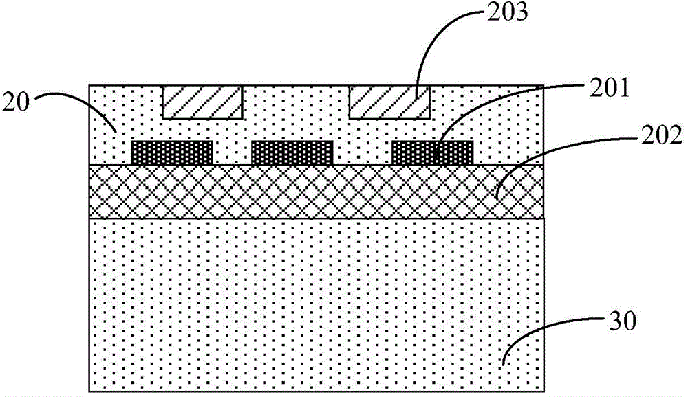
[0048] Below, refer to Figures 2A-2D and image 3 The method of the embodiment of the present invention is described in detail. in, Figures 2A-2D It shows a schematic cross-sectional view of the device obtained by sequentially implementing the method according to Embodiment 1 of the present invention; image 3 A flow chart showing the sequential implementation steps of the method in Embodiment 1 of the present invention is shown.

[0049] First, in step 1, a device wafer 20 is provided, and a first bonding interface layer 202 is formed on the front surface of the device wafer 20, such as Figure 2A shown.

[0050]Specifically, components and interconnection structures, such as metal pads 201 , are formed on the front side of the device wafer 20 . In one example, when the device wafer is an IGBT, the front surface structure formed on the front surface of the device wafer 20 includes a base region, an emitter region, a gate oxide layer, a gate electrode, and an emitter el...

Embodiment 2

[0070] The present invention also provides a semiconductor device, which is manufactured by the method described in Embodiment 1. Since the method in the first embodiment does not add other bonding media, the cost is low and the efficiency is high, the manufacturing process is mature and simple, and the method of debonding in the first embodiment is used, and the uniformity is good. Due to the above advantages, the semiconductor device of the present invention has good performance.

Embodiment 3

[0072] The present invention also provides an electronic device, which includes the semiconductor device described in the second embodiment.

[0073] The electronic device also has the above advantages due to the excellent performance of the included semiconductor device.

[0074] The electronic device can be any electronic product or equipment such as mobile phone, tablet computer, notebook computer, netbook, game console, TV, VCD, DVD, navigator, camera, video recorder, voice recorder, MP3, MP4, PSP, etc. It is an intermediate product with the above-mentioned semiconductor device, for example: a mobile phone motherboard with the integrated circuit, etc.


PUM


Abstract

The invention provides a semiconductor device and a manufacturing method thereof, and an electronic apparatus. The manufacturing method comprises the following steps of providing a device wafer and forming a first bonding interface layer on a right side of the device wafer; providing a support wafer and forming a second bonding interface layer on a surface of the support wafer, wherein the support wafer executes hydrogen ion implantation; forming a hydrogen ion implantation layer in an area, wherein a predetermined depth is arranged between the area and the second bonding interface layer; carrying out a bonding technology and making the first bonding interface layer of the device wafer be connected to the second bonding interface layer of the support wafer; carrying out thinning on a back side of the device wafer; executing annealing processing and realizing hydrogen embrittlement fragmentation de-bonding so as to peel most of the support wafer; and removing the residual support wafer. According to the manufacturing method in the invention, other bonding mediums are not needed; cost is low and efficiency is high; the process is mature and simple; by using a de-bonding method, uniformity is good; other tools are not needed; the process is simple and the operability is high.

Description

technical field [0001] The invention relates to the technical field of semiconductors, in particular to a semiconductor device, a manufacturing method thereof, and an electronic device. Background technique [0002] In semiconductor technology, an insulated gate bipolar transistor (Insulated Gate Bipolar Transistor, referred to as IGBT) is a composite full-control voltage-driven power semiconductor device composed of a bipolar transistor (BJT) and an insulated gate field effect transistor (MOSFET). It has the advantages of high input impedance of MOSFET and low turn-on voltage drop of power transistor (Giant Transistor, referred to as GTR). Therefore, IGBT is widely used in frequency converters and inverters as a necessary switching device. in the circuit structure. [0003] In order to reduce energy loss and improve heat dissipation, it is often necessary to thin the IGBT device. However, the thinner the wafer is, the more likely it is to crack and deform during transmissi...

Claims


Application Information

Patent Timeline
IPC IPC(8): H01L29/739H01L21/336H01L29/78
Inventor 施林波陈福成侯飞凡
Owner SEMICON MFG INT (SHANGHAI) CORP
Why Eureka
Try Eureka