Semiconductor silicon wafer, flattening method therefor, preparation method therefor, and semiconductor device

A planarization method and semiconductor technology, applied in semiconductor devices, semiconductor/solid-state device manufacturing, electrical components, etc., can solve the problems of semiconductor device leakage, incomplete grinding, and silicon nitride can not be completely corroded, so as to improve planarization degree of effect

Active Publication Date: 2016-03-16
FOUNDER MICROELECTRONICS INT
View PDF5 Cites 3 Cited by
  • Summary
  • Abstract
  • Description
  • Claims
  • Application Information

AI Technical Summary

Problems solved by technology

[0008] Embodiments of the present invention provide a semiconductor silicon wafer and its planarization method, preparation method, and semiconductor device to solve the problem in the prior ar

Method used


Image

  • Semiconductor silicon wafer, flattening method therefor, preparation method therefor, and semiconductor device
  • Semiconductor silicon wafer, flattening method therefor, preparation method therefor, and semiconductor device
  • Semiconductor silicon wafer, flattening method therefor, preparation method therefor, and semiconductor device

Examples


Embodiment 1

[0060] Such as figure 2 As shown, it is a schematic flowchart of a semiconductor silicon wafer planarization method provided in Embodiment 1 of the present invention, which mainly includes the following steps:

[0061] Step 201: Using hydrofluoric acid solution or a mixed solution of hydrofluoric acid and ammonium fluoride, etch the silicon oxynitride located on the silicon nitride in the active region of the semiconductor silicon wafer. Wherein, the semiconductor silicon wafer is a silicon wafer formed with a field oxide layer.

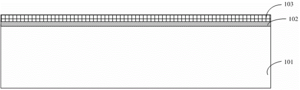
[0062] In the embodiment of the present invention, a semiconductor silicon wafer with a field oxide layer formed as shown in FIG. The semiconductor silicon wafer as shown in FIG. 3(a) is obtained in other ways, and the present invention does not limit its specific implementation, as long as the semiconductor silicon wafer as shown in FIG. 3(a) is obtained.

[0063] Since silicon oxynitride and hydrofluoric acid can react chemically, the nitrogen p...

Embodiment 2

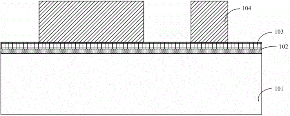
[0078] like Figure 4 As shown, it is a schematic flow chart of a method for preparing a semiconductor silicon wafer provided by Embodiment 2 of the present invention, which specifically includes the following steps:

[0079] Step 301 : forming a pad oxide layer and silicon nitride on the substrate silicon wafer.

[0080] Step 302: Etching the silicon nitride to form a semiconductor silicon wafer including an active region and a field region.

[0081] Step 303: forming a field oxide layer on the field region of the semiconductor silicon wafer including the active region and the field region.

[0082] Step 304: Using hydrofluoric acid solution or a mixed solution of hydrofluoric acid and ammonium fluoride, etch the silicon oxynitride located on the silicon nitride in the active region of the semiconductor silicon wafer.

[0083] Specifically, in this step, the semiconductor silicon wafer is placed in an etching tank, and after the etching time t, the semiconductor silicon waf...

Embodiment 3

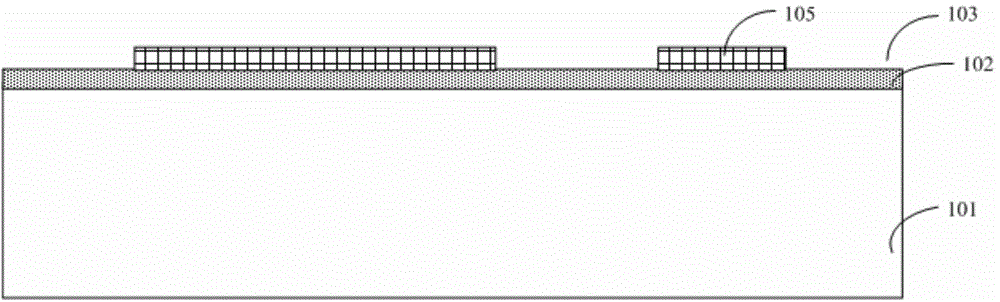
[0089] like Figure 5 As shown, it is a schematic structural diagram of a semiconductor silicon wafer provided by Embodiment 3 of the present invention. In the semiconductor silicon wafer, silicon nitride and silicon oxynitride in the active area are respectively etched away, and the oxide layer in the active area One surface of 501 is fully exposed.

[0090] Wherein, the silicon oxynitride in the active region is corroded by any of the following solutions: a hydrofluoric acid solution with a concentration of 49% hydrofluoric acid and water mixed in a volume ratio of 1:10 to 1:100; A mixed solution of hydrofluoric acid and ammonium fluoride formed by mixing hydrofluoric acid with a concentration of 49% and ammonium fluoride at a volume ratio of 5:1 to 500:1.

[0091] Preferably, the temperature required for the silicon oxynitride in the active region to be etched is 23°C±2°C.


PUM


Abstract

The invention discloses a semiconductor silicon wafer, a flattening method therefor, a preparation method therefor, and a semiconductor device. The flattening method comprises the steps: corroding silicon oxynitride on silicon nitride of an active region in the semiconductor silicon wafer provided with a field oxidation layer through employing hydrofluoric acid solution or the mixed solution of hydrofluoric acid and ammonium fluoride; grinding the surface of the semiconductor silicon wafer through employing the CMP technology, wherein the silicon oxynitride of the semiconductor silicon wafer is corroded; corroding the residual silicon oxynitride on the surface of the ground semiconductor silicon wafer through employing hot phosphoric acid, and obtaining semiconductor silicon chip. Therefore, the method enables all silicon oxynitride in the active region to be corroded before the CMP technology, prevents the incomplete grinding of the silicon oxynitride in the active region of the semiconductor silicon wafer in a smaller area from causing the incomplete corrosion of silicon nitride in a region where there is the residual silicon oxynitride, guarantees that the surface of the active region in the finally obtained semiconductor silicon wafer is completely exposed, and improves the flattening degree of the semiconductor silicon wafer.

Description

technical field [0001] The invention relates to the technical field of semiconductor chips, in particular to a semiconductor silicon wafer, a planarization method, a preparation method and a semiconductor device. Background technique [0002] In the semiconductor process, the local oxidation of silicon (LocalOxideOfSilicon, LOCOS) process is generally used to isolate the semiconductor silicon wafer, that is, a field oxide layer (FieldOxide, FOX) is formed in the field area other than the active area, and finally the active area is isolated. The source region and the field region are used in the preparation of later semiconductor devices. However, the existing LOCOS process will cause the surface of the semiconductor silicon wafer to be uneven. In practice, based on the atomic weight and density of silicon dioxide and silicon, if the thickness of the formed FOX is T, then there will be a FOX of 0.56T raised above the surface of the substrate (monocrystalline silicon). And t...

Claims


Application Information

Patent Timeline
IPC IPC(8): H01L21/306H01L21/311H01L29/06
Inventor 闻正锋马万里赵文魁
Owner FOUNDER MICROELECTRONICS INT
Why Eureka
Try Eureka