AlGaN/GaN heterojunction field effect transistor and preparation method thereof

A heterojunction field effect and transistor technology, which is applied in semiconductor/solid-state device manufacturing, semiconductor devices, electrical components, etc., can solve the problems of difficult device process implementation, unfavorable industrialization promotion, and large damage to crystal quality. The effect of stable and stable transmission ability, avoiding device performance degradation, and strong current transmission ability

Inactive Publication Date: 2016-03-23
FIFTH ELECTRONICS RES INST OF MINIST OF IND & INFORMATION TECH
View PDF9 Cites 11 Cited by
  • Summary
  • Abstract
  • Description
  • Claims
  • Application Information

AI Technical Summary

Problems solved by technology

The epitaxial process of the device structure is also very difficult, and it is difficult to guide the development and production of the actual device. At the same time, the gate Schottky metal in the structure is easy to break down under reverse high voltage, which affects the improvement of the withstand voltage performance of the device.
[0009] From the research and analysis of the above existing technical solutions, from the horizontal conduction structure to the vertical conduction structure, the application of super junction is reflected, but there is no technical s

Method used


Image

  • AlGaN/GaN heterojunction field effect transistor and preparation method thereof
  • AlGaN/GaN heterojunction field effect transistor and preparation method thereof
  • AlGaN/GaN heterojunction field effect transistor and preparation method thereof

Examples


Embodiment

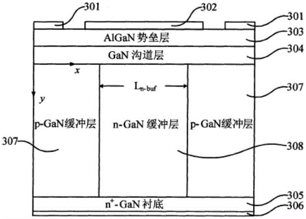
[0049] An AlGaN / GaN heterojunction field effect transistor in this embodiment, such as Figure 4 As shown, it includes a gate 10, a source 8, a drain 11, a substrate 1, an epitaxial structure, and an insulating dielectric layer 9, and the drain 11, the substrate 1, and the epitaxial structure are sequentially stacked;

[0050] The epitaxial structure includes an n-type GaN layer 2, a vertical superjunction layer, a channel layer 4 and a barrier layer 5 stacked in sequence, wherein the vertical superjunction layer includes two lightly doped p-type GaN layers 3, and a heavily doped n-type GaN layer 7 located between two lightly doped p-type GaN layers 3, the thickness of the lightly doped p-type GaN layer 3 is 1 μm to 10 μm, and the doping concentration is 10 16 ~10 17 cm -3 , the thickness of the heavily doped n-type GaN layer 7 is 100 nm to 1 μm smaller than that of the lightly doped p-type GaN layer 3, and the doping concentration is 10 17 ~10 19 cm -3 , the channel laye...


PUM

PropertyMeasurementUnit
Thicknessaaaaaaaaaa
Thicknessaaaaaaaaaa
Doping concentrationaaaaaaaaaa

Abstract

The invention relates to an AlGaN/GaN heterojunction field effect transistor and a preparation method thereof. The field effect transistor comprises a grid, a source, a drain, a substrate, an epitaxial structure and an insulated dielectric layer, wherein the drain, the substrate and the epitaxial structure are orderly arranged in a stacking form; the epitaxial structure comprises a n type GaN layer, a vertical super junction layer, a channel layer and a barrier layer, which are orderly stacked; the vertical super junction layer comprises alternatively arranged light-doped p type GaN layer and heavy-doped n type GaN layer, the heavy-doped n type GaN layer is thinner than the light-doped p type GaN layer, and the channel layer and the barrier layer are stacked on the light-doped p type GaN layer. The field effect transistor is simple in structure; performance deterioration of devices caused by complex device processing is avoided; stability is guaranteed; and relatively high forward current transmission ability and backward high voltage endurance of devices are realized simultaneously.

Description

technical field [0001] The invention relates to a semiconductor device, in particular to an AlGaN / GaN heterojunction field effect transistor and a preparation method thereof. Background technique [0002] In modern society, power electronics technology continues to keep up with new developments, and power electronic devices such as voltage regulators, rectifiers, and inverters are more and more widely used in daily life, involving high-voltage power supply, power management, factory automation, and energy distribution management for motor vehicles. and many other fields. Diodes and switching devices are an integral part of power electronics applications. In recent years, Schottky diodes with high frequency, high current and low power consumption have attracted more and more attention due to their unique performance advantages. [0003] Traditional power Schottky diodes are mainly fabricated on silicon (Si)-based materials. The development of silicon materials has a long h...

Claims


Application Information

Patent Timeline
IPC IPC(8): H01L29/778H01L21/335H01L29/06H01L29/417
CPCH01L29/7788H01L29/0634H01L29/41741H01L29/66431
Inventor 贺致远黄林轶胡坚耀徐华伟
Owner FIFTH ELECTRONICS RES INST OF MINIST OF IND & INFORMATION TECH
Why Eureka
Try Eureka