Double-shoulder-ridge GaAs-based laser preparation method and GaAs-based laser prepared therethrough

A technology of lasers and ridges, applied in lasers, laser parts, semiconductor lasers, etc., can solve the problems of increased raw material consumption, complex process, long production line time, etc., to shorten the production cycle, simplify the process steps, and reduce consumption. Effect

Inactive Publication Date: 2016-03-30
Shandong Huaguang Optoelectronics Co. Ltd.
View PDF5 Cites 3 Cited by
  • Summary
  • Abstract
  • Description
  • Claims
  • Application Information

AI Technical Summary

Problems solved by technology

The steps in the process are complicated, and the production line time is relatively long, which will also increase the probability of abnormal occurrence in the process and increase the consumption of raw materials
Such as the processing method of photoresist disclosed in Chinese patent document CN103309151A and the preparation method of semiconductor devices, the manufacturing method of semiconductor laser disclosed in Chinese patent document CN102299480A just has the technical problems mentioned above, and Chinese patent document CN101154049A provides a kind of preparation The method of glue pattern, this method carries out a large-area exposure by spin-coating a positive photoresist once, and then spin-coats the photoresist again for pattern masking exposure and then develops, and after observing a clear pattern, it is obtained by lengthening the development for a certain period of time Photoresist pattern, which requires multiple photolithography and development, and the process is relatively complicated

Method used


Image

  • Double-shoulder-ridge GaAs-based laser preparation method and GaAs-based laser prepared therethrough
  • Double-shoulder-ridge GaAs-based laser preparation method and GaAs-based laser prepared therethrough
  • Double-shoulder-ridge GaAs-based laser preparation method and GaAs-based laser prepared therethrough

Examples


Embodiment 1

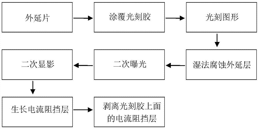
[0034] A kind of preparation method of the GaAs-base laser of double-shoulder ridge bar, comprises steps as follows:

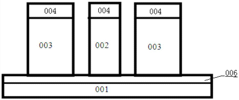
[0035] 1) Etch the epitaxial layer with a double-shoulder structure by photolithography using a photolithography mask, and etch a ridge structure 002 between the double-shoulder structures 003; the tops of the double-shoulder structure 003 and the top of the ridge structure 002 are respectively A photoresist 004 is left; the photolithography method includes steps such as exposure, development, and corrosion;

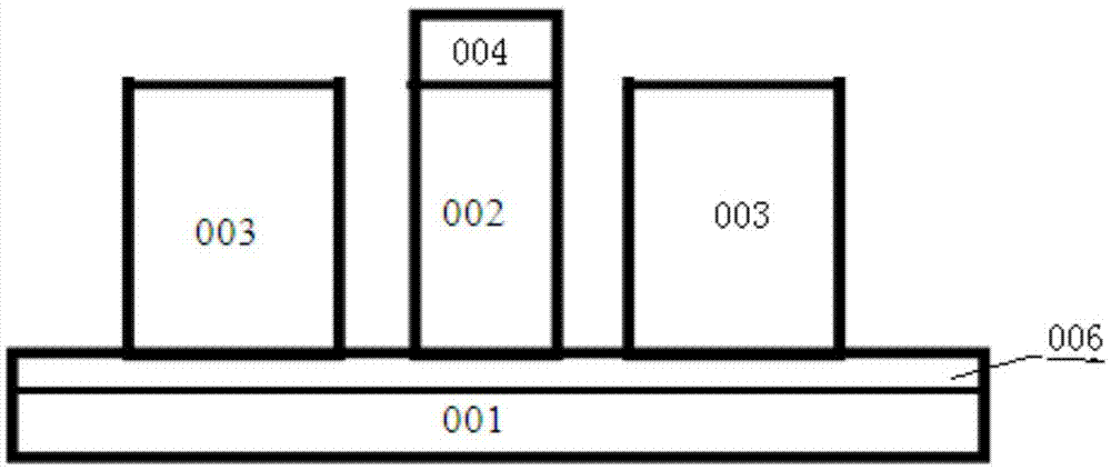
[0036] 2) Second exposure: block the photoresist 004 on the top of the ridge structure 002, and expose the photoresist on the top of the shoulder structure 003;

[0037] 3) Secondary development: remove the photoresist in the exposed part by development;

[0038] 4) growing a current blocking layer 005 on the epitaxial wafer after secondary development;

[0039] 5) Peel off the current blocking layer at the photoresist: peel off the current blocking la...

Embodiment 2

[0045] The preparation method of a kind of GaAs-based laser with double-shouldered ridges as described in Example 1, the difference is that, after the above step 5), it is also necessary to carry out P-face electrode evaporation, thinning, and N-side electrode evaporation on the epitaxial wafer. Electrode evaporation, alloying, packaging and other steps form GaAs-based lasers.

Embodiment 3

[0047] A method for preparing a GaAs-based laser with double-shouldered ridges as described in Example 1, the difference is that in the step 1), the etching of the epitaxial layer is wet etching. The corrosion solution used in the wet etching is a conventional proportion, including a mixture of analytically pure phosphoric acid, hydrogen peroxide, and deionized water, and saturated bromine water; in the mixture of phosphoric acid, hydrogen peroxide, and deionized water , Phosphoric acid: hydrogen peroxide: deionized water=1:1:(3~4) volume ratio.


PUM


Abstract

The invention discloses a double-shoulder-ridge GaAs-based laser preparation method, and the method comprises the following steps: carrying out exposure, development and corrosion through employing a photoetching mask and preparing a needed pattern structure; carrying out secondary exposure; carrying out secondary development; growing a current blocking layer on an epitaxial wafer after the secondary development; peeling the current blocking layer of a photoresist place at the top of a ridge structure, forming a current injection window, carrying out the evaporation and thinning of a P-plane electrode, carrying out the evaporation, alloying and packaging of an N-plane electrode, and forming a GaAs-based laser. The method saves a part of steps in a conventional technology: removing photoresist after corrosion, growing the current blocking layer, and carrying out the pattern corrosion of the current blocking layer in a nesting mode. The method cannot damage to the epitaxial layer on a substrate, is convenient to operate, simplifies the technological steps, shortens the production cycle, and reduces the consumption of raw materials.

Description

technical field [0001] The invention relates to a preparation method of a GaAs-based laser with double-shouldered ridges and a GaAs-based laser prepared by the method, belonging to the technical field of semiconductors. Background technique [0002] Semiconductor laser is a general term for optical oscillators and optical amplifiers produced by stimulated emission of photons caused by semiconductor electron optical transitions. Since the advent of semiconductor lasers, as a new type of light source, they have been favored in various fields due to their own advantages, such as small size, high power, long life, and convenient use. However, there are many steps in the manufacturing process of semiconductor lasers, and the process line is relatively long, especially the photolithography process. The photolithography process uses photoresist to transfer the pattern on the mask plate to the wafer through exposure, development, etc., so that the wafer has the photoresist pattern ...

Claims


Application Information

Patent Timeline
Patent Type & Authority Applications(China)
IPC IPC(8): H01S5/22H01S5/323
CPCH01S5/22H01S5/32316
Inventor 王金翠苏建申国丽徐现刚
Owner Shandong Huaguang Optoelectronics Co. Ltd.
Why Eureka
Try Eureka