
An electrostatic discharge protection device with low trigger voltage

A technology of electrostatic discharge protection and low trigger voltage, which is applied in the field of electrostatic discharge protection device structure, can solve the problems of lower trigger voltage, difficulty in uniform trigger, unsatisfiable uniform trigger conditions, etc., and achieve the effect of low trigger voltage

Active Publication Date: 2018-07-20
SOUTHEAST UNIV
View PDF4 Cites 0 Cited by
  • Summary
  • Abstract
  • Description
  • Claims
  • Application Information

AI Technical Summary

Problems solved by technology

However, high-voltage LDMOS devices exhibit larger snapbacks than low-voltage MOS devices, and the sustain voltage of LDMOS devices is much lower than the trigger voltage.
Although the trigger voltage can be reduced by auxiliary triggering methods such as gate coupling and substrate triggering, there are problems of increasing the complexity of the circuit design and increasing the layout area.
Therefore, under normal circumstances, the multi-finger uniform trigger condition where the failure voltage is greater than the trigger voltage cannot be satisfied, making it more difficult to trigger uniformly than low-voltage multi-finger devices, and there is a serious multi-finger non-uniform turn-on problem that directly affects the on-chip ESD protection capability of high-voltage circuits.

Method used


Image

  • An electrostatic discharge protection device with low trigger voltage
  • An electrostatic discharge protection device with low trigger voltage
  • An electrostatic discharge protection device with low trigger voltage

Examples


Embodiment Construction

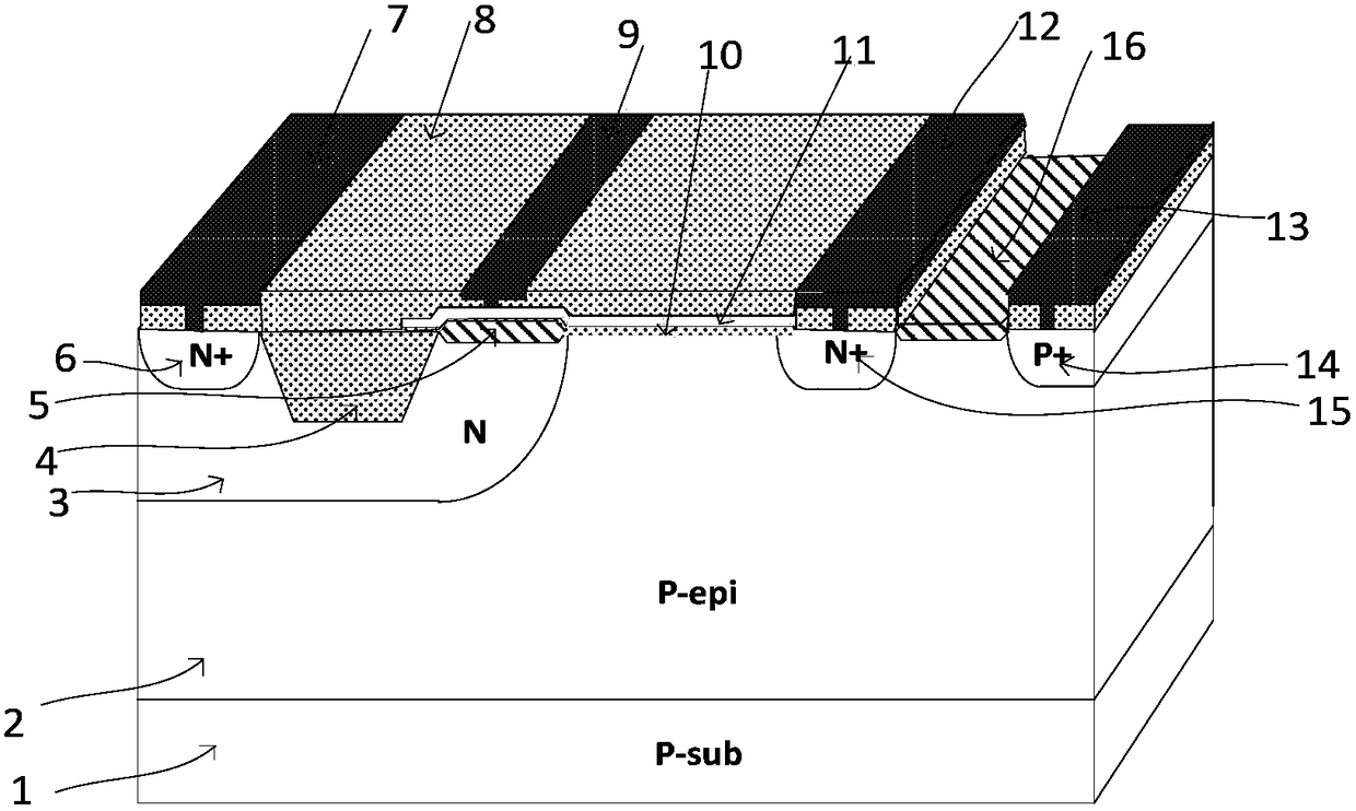
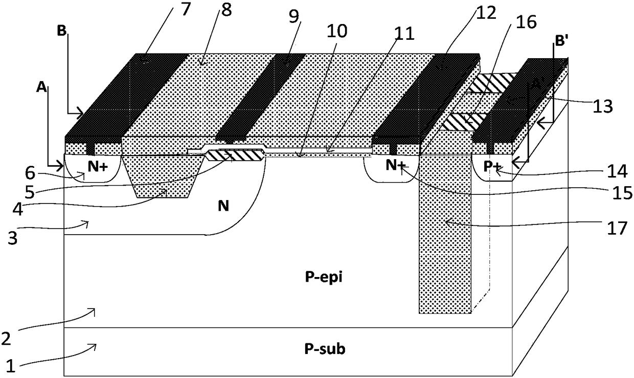
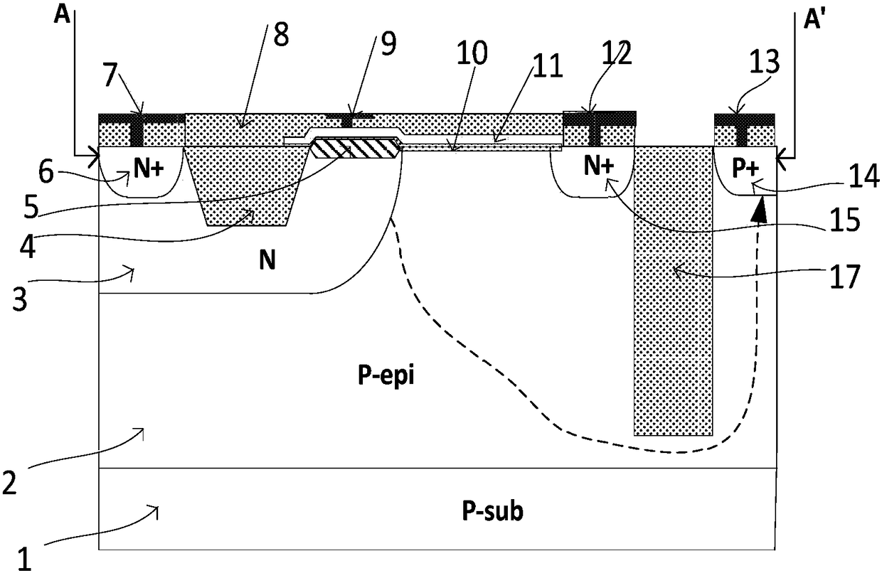
[0020] An electrostatic discharge protection device with a low trigger voltage, comprising: a P-type substrate 1, a P-type epitaxy 2 is arranged above the P-type substrate 1, and an N-type drift region 3 is arranged above the P-type epitaxy 2, N-type drain region 6, shallow trench isolation region 4 and first field oxide layer 5 are arranged in N-type drift region 3, and gate oxide layer 10, N-type source region 15, P Type body region 14, a polysilicon gate 11 is provided above the gate oxide layer 10, and a through passivation layer is respectively provided on the upper surfaces of the N-type drain region 6, the polysilicon gate 11, the N-type source region 15 and the P-type body region 14 8's drain metal contact 7, gate metal contact 9, source metal contact 12 and body metal contact 13, characterized in that a deep The isolation formed by the trench isolation region 17 and the flake field oxide layer 16 and the deep trench isolation region 17 and the flake field oxide layer ...


PUM


Abstract

An electrostatic discharge protection device with low trigger voltage comprises a P-type substrate, wherein a P-type epitaxial layer is arranged on the P-type substrate, an N-type drift region is arranged on the P-type epitaxial layer, an N-type drain region, a shallow slot isolation region and a first field oxide layer are arranged in the N-type drift region, a gate oxide layer, an N-type source region and a P-type body region are further arranged on the P-type epitaxial layer, a poly-silicon gate is arranged on the gate oxide layer, and a drain metal contact, a gate metal contact, a source metal contact and a body region metal contact are respectively arranged on the upper surfaces of the N-type drain region, the poly-silicon gate, the N-type source region and the P-type body region and pass through a passivation layer. The electrostatic discharge protection device is characterized in that isolation means comprising deep slot isolation regions and sheet-shaped field oxide layers are arranged between the N-type source region and the P-type body region, and the deep slot isolation regions and the sheet-shaped field oxide layers are arranged at intervals. By the electrostatic discharge protection device, the trigger voltage of the device can be reduced, the secondary breakdown current is increased, and the robustness of the device during the electrostatic discharge (ESD) process is improved.

Description

technical field [0001] The invention relates to the reliability field of integrated circuits, and relates to an electrostatic discharge protection device structure with low trigger voltage. Background technique [0002] With the improvement of integration and the reduction of device feature size, how to ensure the reliability of devices has become more and more important. According to statistics, electrical overstress (EOS) and electrostatic discharge (ESD) damage account for about 40% of the failure factors of related semiconductor integrated circuits. The reason is that the high electric field or instantaneous high current caused by electrostatic discharge and electrical overstress will cause local overheating of the device, causing breakdown of the dielectric layer, burning of polysilicon or metal wiring, destruction of the passivation layer, and secondary heat generation of the PN junction and even the device. Breakdown, even melting the silicon die and other issues. T...

Claims


Application Information

Patent Timeline
Patent Type & Authority Patents(China)
IPC IPC(8): H01L27/02
CPCH01L27/0259
Inventor 孙伟锋袁永胜叶然魏家行薛颖刘斯扬陆生礼时龙兴
Owner SOUTHEAST UNIV
Learn More