P-type oxide semiconductor thin-film transistor and preparing method thereof

A technology for oxide semiconductors and thin film transistors, applied in the fields of semiconductor/solid-state device manufacturing, transistors, semiconductor devices, etc., can solve the problems of less reports of P-type oxide thin film transistors, and achieve suitable for large-scale industrial production, good electrical properties, Easy-to-use effects

Inactive Publication Date: 2016-04-13
HENAN UNIVERSITY
View PDF2 Cites 5 Cited by
  • Summary
  • Abstract
  • Description
  • Claims
  • Application Information

AI Technical Summary

Problems solved by technology

[0003] However, most oxide semiconductors have intrinsic N-type conductivity, so the oxide thin film transistors cur

Method used


Image

  • P-type oxide semiconductor thin-film transistor and preparing method thereof
  • P-type oxide semiconductor thin-film transistor and preparing method thereof
  • P-type oxide semiconductor thin-film transistor and preparing method thereof

Examples


Embodiment 1

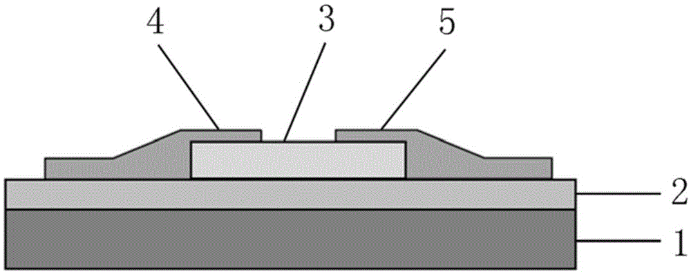
[0033] The P-type oxide semiconductor thin film transistor of this embodiment, such as figure 1 shown, including:

[0034] A substrate 1, the substrate 1 is a heavily doped silicon substrate (heavily doped N-type silicon wafer), and the heavily doped silicon substrate is used as a gate electrode at the same time;

[0035] an insulating layer 2, which is a silicon dioxide film, located on the gate electrode;

[0036] The active layer 3 is a P-type delafossite structure oxide film, located on the insulating layer 2;

[0037] The source electrode 4 and the drain electrode 5 are all Cu films, respectively located on the active layer 3;

[0038] Wherein, the material of the P-type delafossite structure oxide film is CuAlO 2 .

[0039] The thickness of the insulating layer is 300nm, the thickness of the active layer is 80nm, and the thickness of the source electrode and the drain electrode is 200nm.

[0040] The preparation method of the P-type oxide semiconductor thin film tra...

Embodiment 2

[0048] The structure diagram of the P-type oxide semiconductor thin film transistor of this embodiment is the same as that of Embodiment 1, specifically including:

[0049] A substrate, the substrate is a heavily doped silicon substrate (heavily doped N-type silicon wafer), and the heavily doped silicon substrate is used as a gate electrode at the same time;

[0050] an insulating layer, which is a transparent zirconium dioxide film, located on the gate electrode;

[0051] The active layer is a P-type delafossite structure oxide film and is located on the insulating layer;

[0052] The source electrode and the drain electrode are all Cu films, respectively located on the active layer;

[0053] Wherein, the material of the P-type delafossite structure oxide film is CuInO 2 .

[0054] The thickness of the insulating layer is 300nm, the thickness of the active layer is 120nm, and the thickness of the source electrode and the drain electrode is 200nm.

[0055] The preparation ...

Embodiment 3

[0062] The structure diagram of the P-type oxide semiconductor thin film transistor of this embodiment is the same as that of Embodiment 1, specifically including:

[0063] A substrate, the substrate is a heavily doped silicon substrate (heavily doped N-type silicon wafer), and the heavily doped silicon substrate is used as a gate electrode at the same time;

[0064] an insulating layer, which is a transparent aluminum oxide film, located on the gate electrode;

[0065] The active layer is a P-type delafossite structure oxide film and is located on the insulating layer;

[0066] The source electrode and the drain electrode are all Cu films, respectively located on the active layer;

[0067] Wherein, the material of the P-type delafossite structure oxide film is CuGaO 2 .

[0068] Wherein, the thickness of the insulating layer is 300nm, the thickness of the active layer is 120nm, and the thickness of the source electrode and the drain electrode is 200nm.

[0069] The prepar...


PUM

PropertyMeasurementUnit
Thicknessaaaaaaaaaa
Thicknessaaaaaaaaaa
Thicknessaaaaaaaaaa

Abstract

The invention discloses a P-type oxide semiconductor thin-film transistor and a preparing method thereof. The thin-film transistor comprises the components of a heavily doped silicon substrate which is used as a gate electrode; an insulating layer which is an insulating oxide film and is arranged on the gate electrode; an active layer which is a P-type delafossite-structured oxide film and is arranged on the insulating layer; a source electrode and a drain electrode which are Cu films and are arranged on the active layer. The P-type delafossite-structured oxide film is made of CuAlO2, CuInO2 or CuGaO2. The P-type delafossite-structured oxide film which is used as the active layer represents a stable P-type semiconductor characteristic, thereby realizing large valence band maximum frequency bandwidth and high hole mobility. The p-type oxide semiconductor thin-film transistor has a simple structure and furthermore the preparing process of the p-type oxide semiconductor thin-film transistor is compatible with microelectronic technology. Furthermore the p-type oxide semiconductor thin-film transistor has advantages of high chemical stability and excellent electrical property. The p-type oxide semiconductor thin-film transistor has a wide application prospect in organic light-emitting diode displaying, complementary oxide semiconductor electronic circuits and transparent electronic circuits.

Description

technical field [0001] The invention belongs to the technical field of thin film transistors, and in particular relates to a P-type oxide semiconductor thin film transistor, and also relates to a preparation method of the P-type oxide semiconductor thin film transistor. Background technique [0002] Thin film transistor is a unipolar semiconductor device that transmits current by majority carriers, and the semiconductor active layer has a crucial impact on device performance and manufacturing cost. With the continuous emergence of new processes, new materials, and new structures, new thin-film transistors are not only used in active matrix display devices, but also in fields such as thin-film integrated circuits, photoelectric image sensors, thin-film memories, and gas sensors. In recent years, thin-film transistors with oxide semiconductors as the active layer have attracted widespread attention. This type of device has the advantages of high mobility, low preparation tempe...

Claims


Application Information

Patent Timeline
IPC IPC(8): H01L29/786H01L29/24H01L21/34
CPCH01L29/7869H01L29/24H01L29/66969
Inventor 张新安赵俊威李爽张伟风
Owner HENAN UNIVERSITY
Why Eureka
Try Eureka