A probe in a scanning probe microscope, its preparation method and detection method

A scanning probe and detection method technology, applied in the probe field of scanning probe microscope, can solve problems such as inability to perform magneto-thermal, electro-thermal, obtaining single thermal information, and restricting in-depth understanding and research.

Active Publication Date: 2018-10-19
NINGBO INST OF MATERIALS TECH & ENG CHINESE ACADEMY OF SCI
View PDF13 Cites 0 Cited by
  • Summary
  • Abstract
  • Description
  • Claims
  • Application Information

AI Technical Summary

Problems solved by technology

[0005] So far, although people have developed micro-area thermal imaging technology based on scanning probe microscopy, only a single thermal information can be obtained by using this technology, and other physical information such as magnetic domain structure cannot be obtained in situ, synchronously and in real time. , ferroelectric / piezoelectric domain structure, conductive domain structure, etc., cannot perform magnetic-thermal, electric-thermal, or magnetic-electric-thermal coupling imaging, thus limiting the in-depth understanding of the physical mechanism of heat generation and heat dissipation in materials

Method used


Image

  • A probe in a scanning probe microscope, its preparation method and detection method
  • A probe in a scanning probe microscope, its preparation method and detection method
  • A probe in a scanning probe microscope, its preparation method and detection method

Examples


Embodiment 1

[0123] In this embodiment, the scanning probe microscope includes a scanning probe microscope platform, a probe, an electrical signal application unit, a displacement or vibration signal acquisition unit, a thermal signal acquisition unit, an electrical signal acquisition unit, and a central control unit. The probe control unit is used to drive or control the probe to move and / or vibrate. Central control unit: used to initialize each unit of the system, control each unit of the system, receive the shape, heat, and electrical signals of the sample, and obtain the shape, heat, and electrical signal images of the sample after analysis;

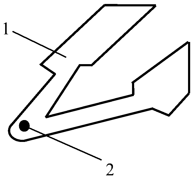
[0124] Such as figure 1As shown, the probe includes a probe arm 1 and a needle tip 2 .

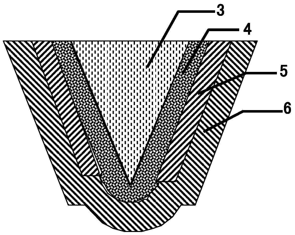
[0125] The structure of needle tip 2 is as follows figure 2 As shown, it is composed of the needle tip body 3 and the surface covering layer. The surface covering layer is composed of film one 4 , film one 4 covering the surface of film two 5 , and film tw...

Embodiment 2

[0149] In this embodiment, the structure of the scanning probe microscope is exactly the same as that in Embodiment 1.

[0150] The difference is that the probe tip with a thermocouple structure is prepared by another method, which includes the following steps:

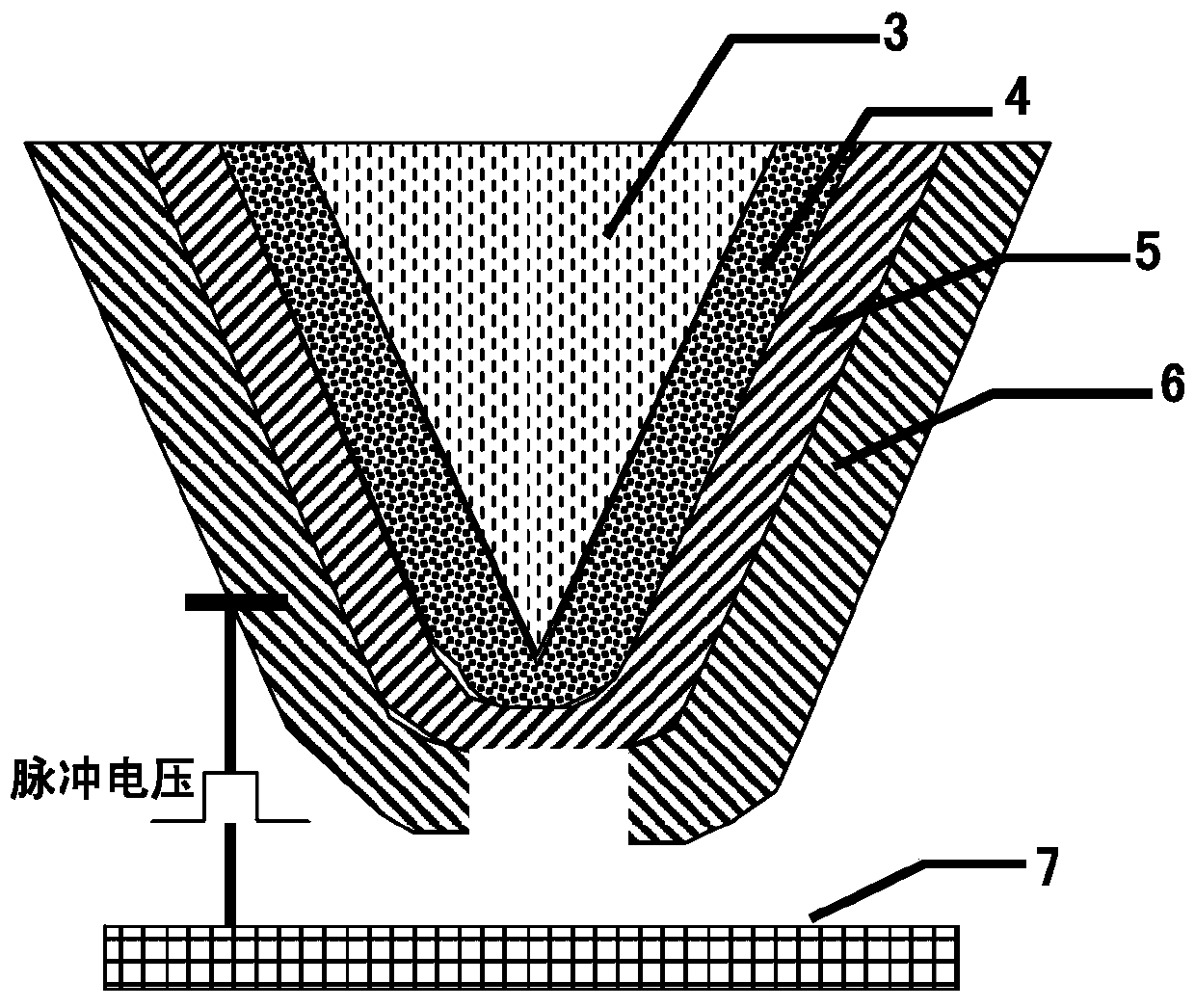
[0151] Step 1. Using the coating method, film one 4, film two 5 and film three 6 are sequentially prepared on the surface of the needle tip body 3;

[0152] Step 2. Apply a voltage between the film 3 6 and the electrode layer 7, and use the tip discharge principle to adjust the distance between the film 3 6 and the electrode layer 7 to melt the film 3 6 at the tip of the needle point, exposing the film 2 5, and Other parts of the film 36 are not melted;

[0153] Step 3: remove the exposed film 2 5 described in step 2, and expose the film 1 4;

[0154] Step 4: Coating the exposed part with the same material as thin film three 6, so that thin film one 4 and thin film three 6 are connected at the tip of the needle tip ...

Embodiment 3

[0157] In this embodiment, the structure of the scanning probe microscope is basically the same as that in Embodiment 1, except that a probe with a thermal resistance structure is used.

[0158] Such as figure 1 As shown, the probe includes a probe arm 1 and a needle tip 2 . Tip 2 as Figure 4 As shown, it includes a needle point body 3, a thermal resistance material layer 8, a first conductive layer 9 and a second conductive layer 10; the thermal resistance material layer 8 is located on the surface of the needle point body 3, and the second conductive layer 10 is located on the surface of the thermal resistance material layer; A conductive layer 9 is in electrical communication with the thermal resistance material layer 8 .

[0159] The thermal resistance material layer 8 is made of low-doped silicon with a thickness of 2m, and the conductive layer 9 is made of bismuth (Bi), nickel (Ni), cobalt (Co), potassium (K), graphite, and graphene. , the thickness is 1 μm, the mate...


PUM


Abstract

The invention provides a probe for a scanning probe microscope. The probe is formed by a probe arm and a probe pointer, wherein the probe pointer is formed by a probe pointer body, a film 1, a film 2 and a film 3 which are arranged on the surface of the probe pointer successively; the film 1 is provided with conductivity; the film 2 is provided with electrical insulating properties; the film 3 is provided with magnetism and conductivity or the film 3 is provided with conductivity; the material of the film 1 is different from the material of the film 3; and the film 1, the film 2 and the film 3 form a thermocouple structure. The probe can be used for in-situ representation for magnetism-electricity-heat multi-parameter of multi-function materials so as to visually research the coupling rule and mechanism between electricity-heat, magnetism-heat and magnetism-electricity-heat of the materials in situ.

Description

technical field [0001] The invention relates to a probe of a scanning probe microscope, in particular to a multi-parameter coupled microscope probe, a preparation method and a detection method thereof. Background technique [0002] With the rapid development of nanoscience and technology, measurement techniques for nanomaterials have emerged, the most notable of which is Scanning Probe Microscopy (STM) technology. [0003] Scanning Probe Microscope (STM) technology is developed based on Scanning Tunneling Microscope (SPM). It has many advantages such as high spatial resolution, and can work in various environments such as vacuum, atmosphere, and even solution, etc., and is widely used. In physics, chemistry, biology, electronics and other research fields. Scanning probe microscopy is to study the corresponding sample properties by detecting the interaction force or physical quantity between the probe and the sample. Currently, it includes atomic force microscope, magnetic f...

Claims


Application Information

Patent Timeline
Patent Type & Authority Patents(China)
IPC IPC(8): G01Q60/16G01Q60/10
Inventor 陈斌李润伟刘宜伟王保敏
Owner NINGBO INST OF MATERIALS TECH & ENG CHINESE ACADEMY OF SCI
Why Eureka
Try Eureka