NLDMOS device and manufacture method thereof

A manufacturing method and device technology, applied in semiconductor/solid-state device manufacturing, semiconductor devices, electrical components, etc., can solve problems such as low on-resistance, reduce device breakdown voltage, etc., achieve large relative permittivity, improve breakdown Voltage, the effect of reducing the electric field strength

Active Publication Date: 2016-04-20
SHANGHAI HUAHONG GRACE SEMICON MFG CORP
View PDF5 Cites 4 Cited by
  • Summary
  • Abstract
  • Description
  • Claims
  • Application Information

AI Technical Summary

Problems solved by technology

In order to make high-performance LDMOS, it is usually necessary to add an additional N-type implant in the drift region of the device to make the device have a lower on-resistance, and this method will reduce the breakdown voltage of the device

Method used


Image

  • NLDMOS device and manufacture method thereof
  • NLDMOS device and manufacture method thereof
  • NLDMOS device and manufacture method thereof

Examples


Embodiment Construction

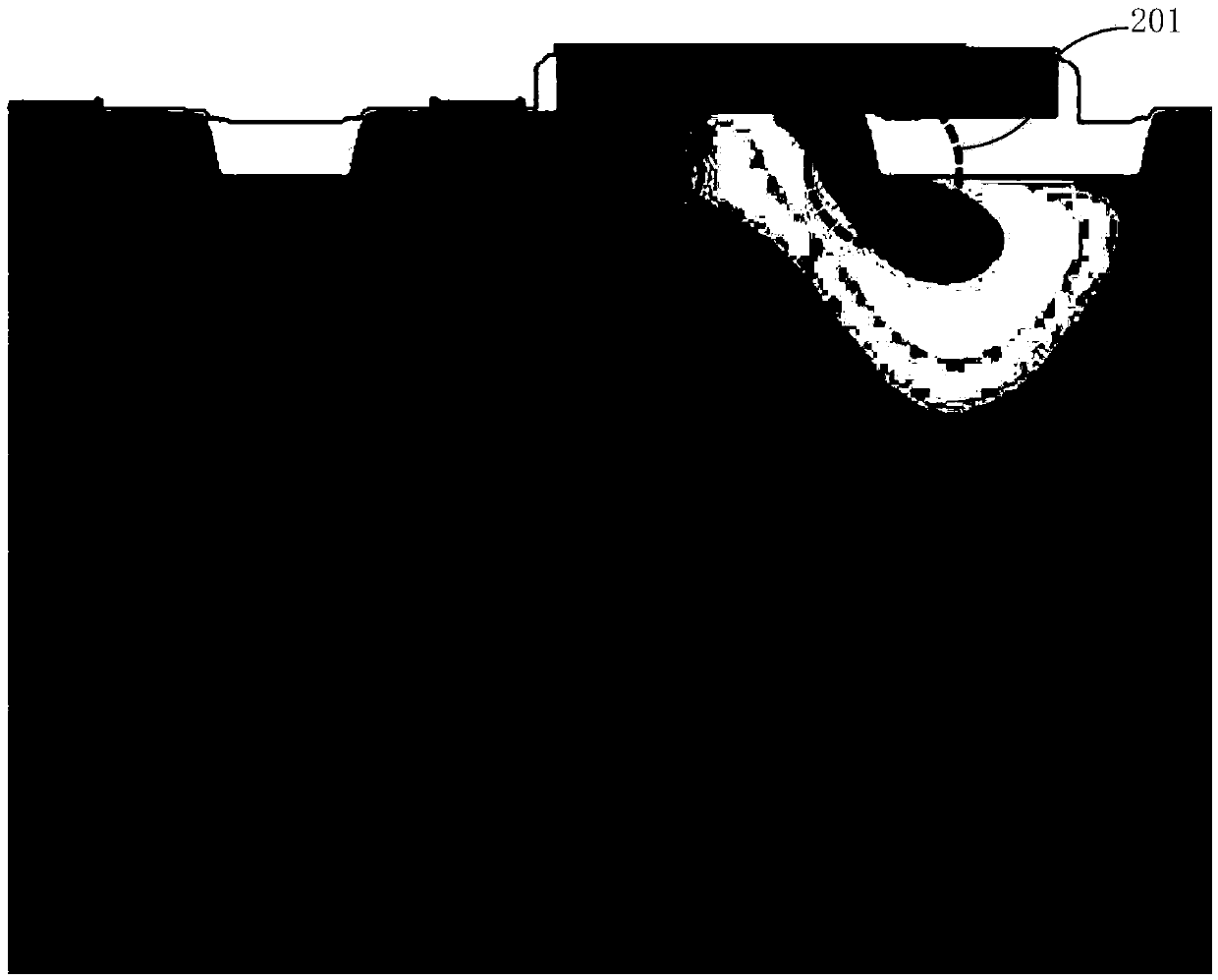
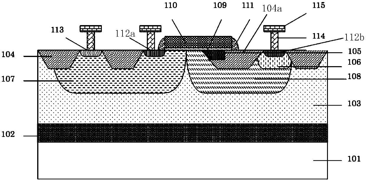
[0047] Such as figure 2 Shown is a schematic structural diagram of the NLDMOS device of the embodiment of the present invention; the NLDMOS device of the embodiment of the present invention includes:

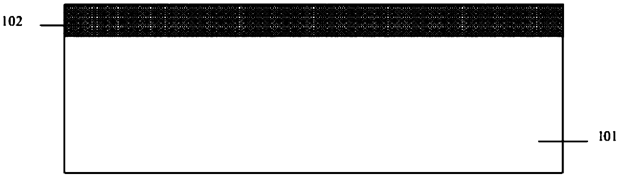
[0048] The N-type doped drift region 108 is formed in the P-type semiconductor substrate 101 . Preferably, the semiconductor substrate 101 is a silicon substrate. A P-type epitaxial layer 103 is formed on the surface of the P-type semiconductor substrate 101, an N-type buried layer 102 is formed at the bottom of the P-type epitaxial layer 103, and the drift region 108 and the subsequent P well 107 are all formed in the P-type epitaxial layer 103. In the P-type epitaxial layer 103.

[0049] The P-well 107 is formed in the P-type semiconductor substrate 101 , and the side of the P-well 107 and the drift region 108 are in contact or separated by a certain distance.

[0050] The polysilicon gate 110 formed above the semiconductor substrate 101, the polysilicon gate 110 is isolat...


PUM


Abstract

The invention discloses an N-type Laterally Diffused Metal Oxide Semiconductor (NLDMOS) device including the following steps that: a field oxide is formed above a drift region, a second side of the drift region field oxide is in lateral contact with a drain region; a first side of the drift region field oxide is arranged at the bottom of a polycrystalline silicon gate, and the first side of the drift region field oxide and a P well are separated by a distance; part of the field oxide at a top region of the first side of the drift region field oxide is removed, and the region where the field oxide is removed is filled with a substitute dielectric layer which has a character that the capacity for blocking ion implantation of the substitute dielectric layer is larger than that of the field oxide or a relative dielectric constant of the substitute dielectric layer is larger than that of the field oxide; and by using the character of the large capacity for blocking the ion implantation, the substitute dielectric layer makes a doping concentration of the drift region at the bottom of the first side of the drift region field oxide lower, thereby improving a breakdown voltage of the NLDMOS device, and by using the character of the large relative dielectric constant, the substitute dielectric layer makes the electric field strength at the bottom of the first side of the drift region field oxide reduce, thereby improving the breakdown voltage of the NLDMOS device. The invention also discloses a manufacture method of the NLDMOS device.

Description

technical field [0001] The invention relates to the field of semiconductor integrated circuit manufacturing, in particular to an N-type laterally diffused metal oxide semiconductor (NLDMOS) device; the invention also relates to a manufacturing method of the NLDMOS device. Background technique [0002] In LDMOS devices, on-resistance is an important indicator. In order to make high-performance LDMOS, it is usually necessary to add an additional N-type implant in the drift region of the device to make the device have a lower on-resistance, and this method will reduce the breakdown voltage of the device. For process platforms with a size below 180nm, the isolation structure of LDMOS is shallow trench field oxygen (STI) isolation. When breakdown occurs, the corner of STI is the strongest point of impact ionization, where the electric field intensity is the highest. In order to improve the breakdown voltage of the device , it is necessary to reduce the doping concentration in th...

Claims


Application Information

Patent Timeline
IPC IPC(8): H01L29/78H01L21/336H01L29/06
CPCH01L29/0603H01L29/66681H01L29/7816
Inventor 石晶钱文生刘冬华胡君段文婷
Owner SHANGHAI HUAHONG GRACE SEMICON MFG CORP
Why Eureka
Try Eureka