A kind of chemical etching method of bismuth selenide material

A chemical etching and bismuth selenide technology is applied in the field of chemical etching of bismuth selenide materials, and can solve the problems of deviation of the surface of bismuth selenide materials from stoichiometric ratio, difficulty in obtaining an etching interface, and excessive etching rate. , to achieve the effect of convenient etching rate, etching rate control, and simple process

Active Publication Date: 2017-10-27
UNIV OF ELECTRONICS SCI & TECH OF CHINA
View PDF7 Cites 0 Cited by
  • Summary
  • Abstract
  • Description
  • Claims
  • Application Information

AI Technical Summary

Problems solved by technology

[0003] However, there are certain technical limitations when using existing etchant to etch BiSe Bismuth oxide is used to etch the surface to reveal the morphology of defect etch pits; the second type - aqua regia etchant has the problems of too fast etching rate and uneven etching, and it is difficult to obtain a flat etching interface. Especially when etching bismuth selenide thin film materials, the etching rate at the film and substrate interface is too fast and easily causes the film layer to fall off; the (3) class——etching agent can obtain a smooth etching interface and can However, our recent research has found that with the different types of acid solutions in the potassium dichromate etchant, the etching rates of selenium and bismuth components are quite different, so it is easy to cause selenization as the etching progresses. Surface deviation of bismuth material from stoichiometric ratio

Method used


Image

  • A kind of chemical etching method of bismuth selenide material
  • A kind of chemical etching method of bismuth selenide material
  • A kind of chemical etching method of bismuth selenide material

Examples


Embodiment 1

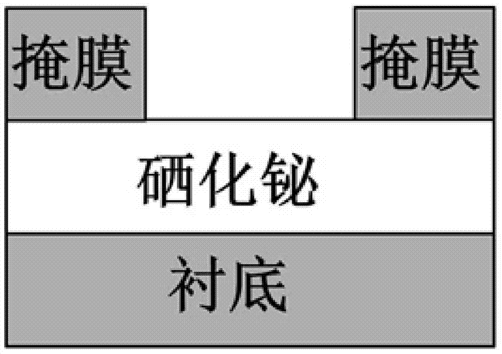
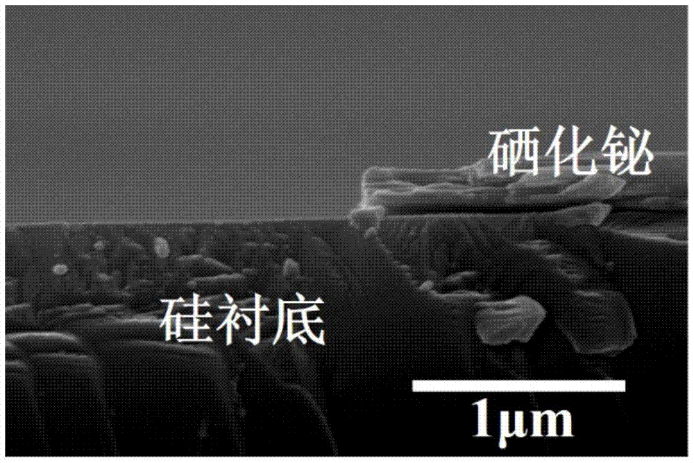
[0018] Embodiment 1: a kind of method that the epitaxial bismuth selenide single crystal thin film on the silicon substrate is etched, at first use standard photolithography technique to make on the bismuth selenide single crystal thin film epitaxial on the silicon substrate figure 2 The mask is shown, and the thickness h' of the mask is measured by a step meter; then potassium dichromate with a molar concentration of 0.02mol / L and a solution of concentrated sulfuric acid and concentrated hydrochloric acid with a volume ratio of 1.5:1 are used to prepare Potassium dichromate complex acid solution; use potassium dichromate complex acid solution to etch for 25 seconds, and measure the thickness h of the mask after etching with a step meter. Experiments have proved that the potassium dichromate compound acid solution has no corrosive effect on the mask, so h-h' is the thickness of etching. The etching was carried out stably at a speed of 150 nm / min, and finally a flat surface wa...

Embodiment 2

[0019] Embodiment 2: A kind of method is carried out etching bismuth selenide single crystal flake after cleavage, at first use standard photolithography technique to make on the bismuth selenide single crystal flake after cleaving figure 2 Shown mask, then with the potassium dichromate that molar concentration is 0.03mol / L, the concentrated sulfuric acid and the concentrated hydrochloric acid solution that volume ratio is 1.5:1, make potassium dichromate compound acid solution; Use dichromate The potassium compound acid solution was etched for 30 seconds, and the etching thickness was measured to be 120nm by using a step meter, and the etching rate was obtained to be 60nm / min, and finally a flat surface was obtained on the surface of the bismuth selenide single crystal.

Embodiment 3

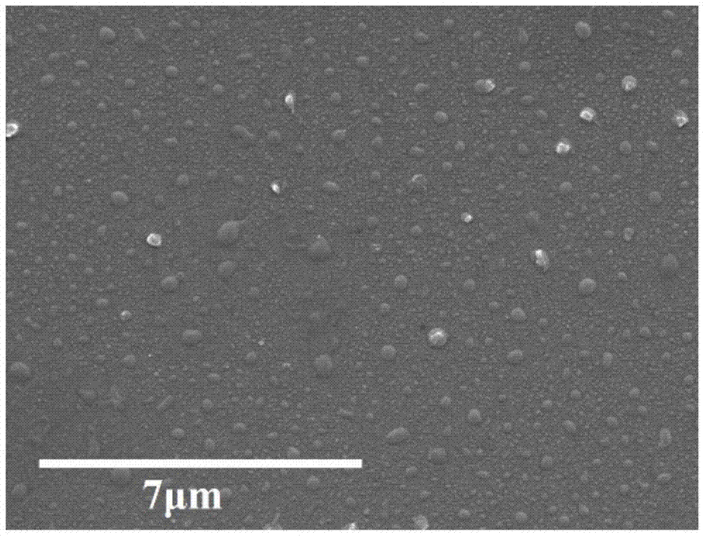
[0020] Embodiment 3: a kind of method that the bismuth selenide single crystal thin film epitaxial on silicon substrate (film thickness 300nm) is etched, at first use standard photolithography technique on the bismuth selenide single crystal thin film epitaxial on silicon substrate made as figure 2 Shown mask, then with the potassium dichromate that molar concentration is 0.012mol / L, the concentrated sulfuric acid and the concentrated hydrochloric acid solution that volume ratio is 1.5:1, make potassium dichromate compound acid solution; Use dichromate After the potassium compound acid solution was etched for 20 seconds, the etching thickness was measured to be 150 nm, and the etching rate was obtained to be 450 nm / min. A flat surface was obtained on the surface of the bismuth selenide single crystal, and the surface did not deviate from the stoichiometric ratio as measured by EDS.

[0021] The above method for etching intrinsic bismuth selenide material is also applicable to...


PUM


Abstract

The present invention relates to a chemical etching method for bismuth selenide material, which comprises the following steps: (1) making a mask: the mask is a photolithography mask, which is made by standard photolithography technology and attached to a silicon substrate (2) preparation of etchant: the etchant is a potassium dichromate complex acid solution, and its preparation method is that the following components are mixed according to a certain proportion, and the volume percentage Be 9% potassium dichromate saturated aqueous solution, the concentrated hydrochloric acid that volume percentage is 48%, the concentrated sulfuric acid that volume percentage is 98%; (3) etching: utilize the potassium dichromate compound acid solution that step (3) makes The etchant is used to etch the bismuth selenide material attached to the photolithography mask prepared in the attaching step (1). The invention has the advantages of simple process, convenient operation, low cost and remarkable effect. The surface of the etched bismuth selenide material is smooth, conforms to the stoichiometric ratio, and the etching rate is easy to control.

Description

technical field [0001] The invention relates to a chemical etching method for bismuth selenide material. Background technique [0002] Bismuth selenide (Bi 2 Se 3 ) is a traditional thermoelectric material. In recent years, studies have found that it is a strong topological insulator quantum material, and its bulk energy band gap is wide (~0.3eV). It is one of the topological insulator materials that are most likely to be applied at room temperature. Etching is a very necessary step in the process of making bismuth selenide into various thermoelectric energy devices and micro quantum devices. At present, the etching technology is mainly divided into dry etching and wet etching. The plasma equipment required for dry etching is expensive, the operation is complicated, and there is no selectivity to the etching of materials, so the damage to the mask is relatively large. Large; wet etching is divided into electrochemical etching and chemical etching, etc. Among them, chemica...

Claims


Application Information

Patent Timeline
Patent Type & Authority Patents(China)
IPC IPC(8): C30B33/10C30B29/46
CPCC30B29/46C30B33/10
Inventor 李含冬张忠阳高磊任武洋李勇龙城佳姬海宁戴丽萍周志华巫江牛晓滨王志明
Owner UNIV OF ELECTRONICS SCI & TECH OF CHINA
Why Eureka
Try Eureka