Semiconductor device, preparation method and packaging method thereof

A packaging method and semiconductor technology, applied in the direction of semiconductor devices, semiconductor/solid-state device manufacturing, semiconductor/solid-state device components, etc., can solve problems affecting wafer bonding strength, etc., to improve weak current problems, improve bonding quality, Effect of improving package reliability

Inactive Publication Date: 2016-05-11
SEMICON MFG INT (SHANGHAI) CORP
View PDF3 Cites 16 Cited by
  • Summary
  • Abstract
  • Description
  • Claims
  • Application Information

AI Technical Summary

Problems solved by technology

However, the surface of the copper pillar obtained by CPM treatment is usually slightly higher than the oxide (Oxide), resulting i...

Method used


Image

  • Semiconductor device, preparation method and packaging method thereof
  • Semiconductor device, preparation method and packaging method thereof
  • Semiconductor device, preparation method and packaging method thereof

Examples


Embodiment 1

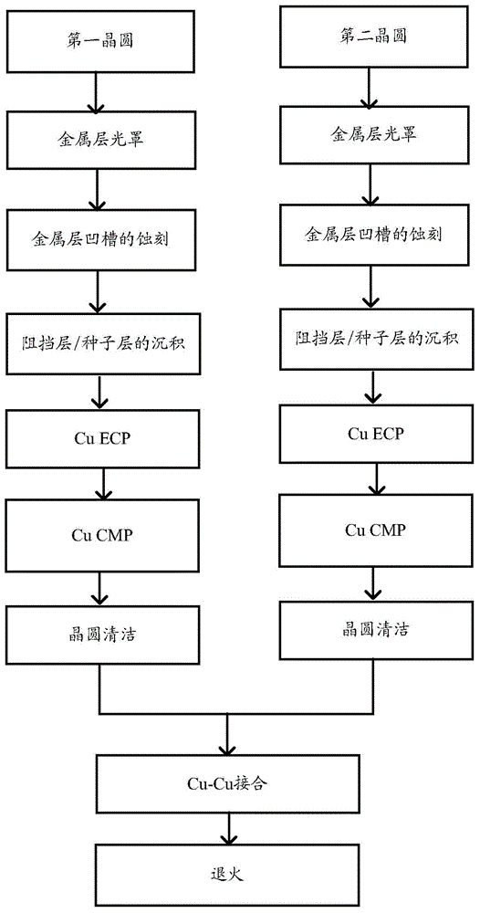
[0057] In order to solve the problems existing in the current wafer bonding process, the present invention provides a method for preparing and packaging a semiconductor device. Figure 4-5 The method is described further.

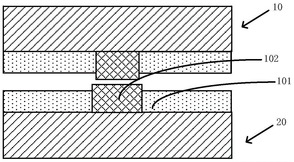
[0058] in, Figure 4 The process flow chart of bonding two wafers in the present invention; Figure 5 It is a schematic diagram of a partial structure of bonding two wafers in a specific embodiment of the present invention.

[0059] Firstly, step 201 is executed to provide a substrate 201 .

[0060] Specifically, refer to Figure 5 , in this step, the base 201 includes at least a substrate, and the substrate may be at least one of the materials mentioned below: silicon, silicon-on-insulator (SOI), stacked silicon-on-insulator (SSOI), Silicon germanium on insulator (S-SiGeOI) and silicon germanium on insulator (SiGeOI) are laminated.

[0061] Optionally, components and interconnection structures may also be formed on the substrate 201 .

[0062] Step 2...

Embodiment 2

[0109] The present invention also provides a semiconductor device, which is prepared by the method described in Embodiment 1. The semiconductor device prepared by the method can realize the hermetic bonding of the bonding pad, increase the bonding strength (bondingstrength), and improve the bonding quality of the wafer; using an insulating AD-BCB material for auxiliary bonding can improve The weak current problem between the joint copper pillars (Cupillar) improves the electrical stability; the use of hybrid bonding (hybrid bonding) can greatly improve the reliability of the package and the life of the chip.

Embodiment 3

[0111] The present invention also provides an electronic device, including the semiconductor device described in Embodiment 2. Wherein, the semiconductor device is the semiconductor device described in Embodiment 3, or the semiconductor device obtained according to the preparation method described in Embodiment 1.

[0112] The electronic device of this embodiment can be any electronic product or equipment such as mobile phone, tablet computer, notebook computer, netbook, game console, TV set, VCD, DVD, navigator, camera, video recorder, voice recorder, MP3, MP4, PSP, etc. , can also be any intermediate product including the semiconductor device. The electronic device according to the embodiment of the present invention has better performance due to the use of the above-mentioned semiconductor device.


PUM

PropertyMeasurementUnit
Thicknessaaaaaaaaaa

Abstract

The invention relates to a semiconductor device, a preparation method and a packaging method thereof. The preparation method comprises the steps of S1, providing a substrate on which an interlayer dielectric layer and a binding pad in the interlayer dielectric layer are formed; S2, forming a photosensitive benzocyclobutene material layer on the interlayer dielectric layer and the binding pad, thereby covering the interlayer dielectric layer and the binding pad; and a step S3, patterning the benzocyclobutene material layer for forming an opening and exposing the binding pad. The semiconductor device, the preparation method and the packaging method are advantageous in that 1, a hybrid bonding process is used for performing sealed bonding on a bond pad (such as a Cu pillar), thereby improving bonding strength and improving bonding quality of a wafer; 2, an AD-BCB material with insulativity is used for performing auxiliary bonding, a problem of weak current between Cu pillars can be settled, and electric stability is improved; and 3, hybrid bonding is utilized, thereby greatly improving packaging stability and prolonging service life of a chip.

Description

technical field [0001] The invention relates to the field of semiconductors, in particular, the invention relates to a semiconductor device, a preparation method and a packaging method. Background technique [0002] In the field of electronic consumption, multi-function devices are more and more popular among consumers. Compared with devices with simple functions, the production process of multi-function devices will be more complicated, such as the need to integrate multiple chips with different functions on the circuit board, so 3D integrated circuit (integrated circuit, IC) technology, 3D integrated circuit (integrated circuit, IC) is defined as a system-level integrated structure, stacking multiple chips in the vertical plane direction, thereby saving space, the edge of each chip can be according to It is necessary to lead out multiple pins, and use these pins to interconnect the chips that need to be connected to each other through metal wires. However, there are still ...

Claims


Application Information

Patent Timeline
IPC IPC(8): H01L23/488H01L21/60
Inventor 施林波陈福成
Owner SEMICON MFG INT (SHANGHAI) CORP
Why Eureka
Try Eureka