Copper pillar bump interconnection structure for directional growth and preparation method of copper pillar bump interconnection structure

An interconnection structure and directional growth technology, which is applied in semiconductor/solid-state device manufacturing, electrical components, electrical solid-state devices, etc., to achieve industrialization, improve interconnection performance and service reliability, and facilitate industrialization

Active Publication Date: 2016-06-01
INST OF METAL RESEARCH - CHINESE ACAD OF SCI
View PDF3 Cites 17 Cited by
  • Summary
  • Abstract
  • Description
  • Claims
  • Application Information

AI Technical Summary

Problems solved by technology

[0006] However, the existing nano-twinned copper preparation technology mainly uses a Ti plate or an amorphous Ni-P film as a cathode plate to prepare a nano-twinned copper bulk material that can be peeled off, which is different from the wafer-based substrate in the microelectronics industry. The process for electroplating is very different, and there is no case of using this high-performance nano-twinned copper in the microelectronics industry

Method used


Image

  • Copper pillar bump interconnection structure for directional growth and preparation method of copper pillar bump interconnection structure
  • Copper pillar bump interconnection structure for directional growth and preparation method of copper pillar bump interconnection structure
  • Copper pillar bump interconnection structure for directional growth and preparation method of copper pillar bump interconnection structure

Examples


Embodiment 1

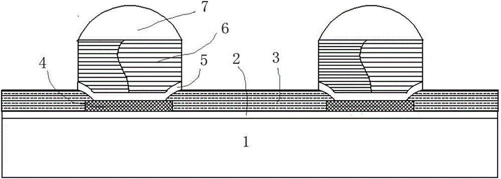
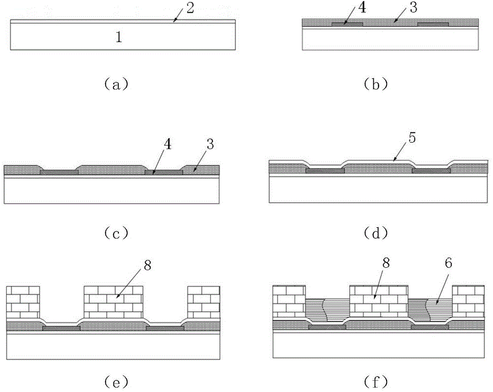
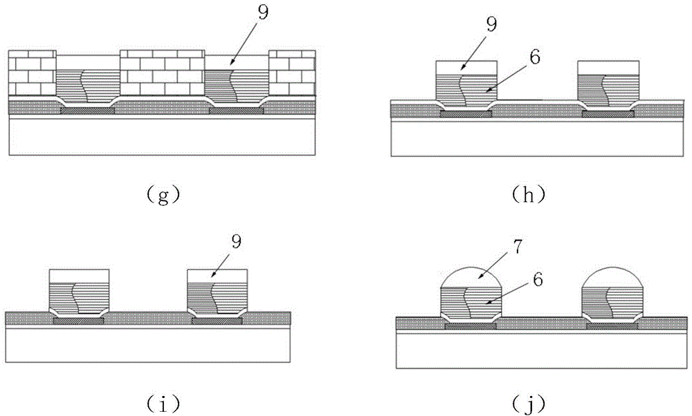
[0054] figure 2 It is a process flow chart for preparing a copper pillar bump interconnection structure of directional growth nano-twinned copper in the present invention, and the process steps are:

[0055] (1) Prepare the wafer base 1 with insulating layer 2, such as figure 2 (a), arranging a metal disc 4 on the insulating layer 2; or directly using a chip on which a metal disc and interconnection lines have been arranged as a substrate;

[0056] (2) deposit dielectric layer 3 on insulating layer 2 and metal plate 4, as figure 2 (b), selectively masking and etching the dielectric layer makes the surface of the metal disk 4 exposed in the window of the dielectric layer 3, such as figure 2 (c);

[0057] (3) Deposit seed layer 5 on dielectric layer 3 and exposed metal disk 4, as figure 2 (d); The method of depositing the seed layer is physical vapor deposition (PVD) or sputtering, etc., the thickness of the seed layer is about 200nm, and the materials are Ti and Cu;

...

Embodiment 2

[0068] This embodiment is a preparation process for a copper pillar bump interconnection structure of directional growth nano-twinned copper, which is different from Embodiment 1 in that: step (5) in the process of direct current electroplating copper pillars: the electroplating solution is composed of: copper sulfate 200g / L, methanesulfonic acid 40mL / L, sodium chloride 30ppm (calculated according to the chlorine content in sodium chloride), polyethyleneimine 5ppm, gelatin 20ppm, and the rest is water; the electroplating anode plate is phosphor copper plate, phosphor copper plate The P element content in the medium is 0.03‐0.075wt.%, and the current density is 40mA / cm 2 , Electromagnetic stirring is used in the electroplating process to ensure that the concentration in the plating solution is uniform.

[0069] The cross-sectional structure of the copper pillars in the copper pillar bump interconnection structure obtained in this embodiment is analyzed, and the result is the sa...


PUM

PropertyMeasurementUnit
thicknessaaaaaaaaaa
thicknessaaaaaaaaaa
thicknessaaaaaaaaaa

Abstract

The invention discloses a copper pillar bump interconnection structure for directional growth and a preparation method of the copper pillar bump interconnection structure, and belongs to the field of microelectronic and microelectromechnical system package. The copper pillar bump interconnection structure comprises a wafer substrate, an insulating layer, metal plates, a dielectric layer, seed layers, copper pillars and solder bumps, wherein each copper pillar contains a nano-twin copper structure for directional growth; and the solder bumps are arranged at the top ends of the copper pillars. The copper pillar bump interconnection structure containing nano-twin copper for directional growth is prepared on the wafer substrate by a traditional DC electroplating technology, so that, on one hand, the interconnection property and the operational reliability of the copper pillar bumps can be improved by excellent characteristics of high strength, high conductivity and the like of the nano-twin copper, and on the other hand, industrialization is relatively easy to achieve by the achievements of the invention due to the fact that the DC electroplating technology can be compatible to an existing wafer level packaging technique.

Description

technical field [0001] The present invention relates to the technical field of packaging of microelectronics and micro-electromechanical systems, in particular to a directional growth copper pillar bump interconnection structure and a preparation method thereof, which prepares directional growth copper pillar bumps on a wafer substrate based on direct current electroplating technology interconnect structure. The method can be applied to the copper pillar bump technology using the copper filling process in the wafer level packaging process. Background technique [0002] In recent years, in the field of microelectronic interconnection, common packaging forms are SIP, CSP or BGA. These packaging technologies have been widely used in computers, mobile phones, and memory devices, but the rapidly developing electronics industry has been seeking a packaging structure that can achieve higher density interconnection in a smaller size. Therefore, copper pillar bump technology and ho...

Claims


Application Information

Patent Timeline
Patent Type & Authority Applications(China)
IPC IPC(8): H01L23/48H01L23/488H01L21/768
CPCH01L2224/11H01L2224/13147
Inventor 刘志权孙福龙李财富祝清省郭敬东
Owner INST OF METAL RESEARCH - CHINESE ACAD OF SCI
Why Eureka
Try Eureka