Supercharge Your Innovation With Domain-Expert AI Agents!

HVMOS integrated with demagnetization sampling device, and demagnetization sampling circuit

A demagnetization sampling and device technology, applied in the field of HVMOS, can solve the problems that the chip demagnetization signal feedback port is susceptible to interference, increase system cost, waste chip area, etc., to save auxiliary windings and voltage divider resistors, reduce system cost, reduce Die area effect

Active Publication Date: 2016-06-08
CRM ICBG (WUXI) CO LTD
View PDF3 Cites 1 Cited by
  • Summary
  • Abstract
  • Description
  • Claims
  • Application Information

AI Technical Summary

Problems solved by technology

The disadvantages of the first type of sampling technology are: (1), the peripheral of the system needs auxiliary windings and voltage divider resistors, which increases the system cost; (2), the chip demagnetization signal feedback port is susceptible to interference
The second type of sampling often uses high-voltage gate-to-drain parasitic capacitance of switching devices for sampling. The disadvantages are: (1) The high-voltage drain-gate parasitic capacitance of switching devices has a relatively small capacitance value, and depletion capacitance will be introduced due to the increase in drain voltage , so that the drain-gate parasitic capacitance is connected in series with the depletion capacitance, so that the equivalent drain-gate capacitance decreases
In order to increase the capacitance value, it is necessary to increase the area of ​​the high-voltage switching device, which seriously wastes the chip area; (2), the gate-drain capacitance forms a series relationship with the gate-source capacitance and the gate-substrate capacitance at the same time. In actual use, the gate-drain capacitance The capacitor is affected and cannot be used as an independent high-voltage capacitor

Method used


Image

  • HVMOS integrated with demagnetization sampling device, and demagnetization sampling circuit
  • HVMOS integrated with demagnetization sampling device, and demagnetization sampling circuit
  • HVMOS integrated with demagnetization sampling device, and demagnetization sampling circuit

Examples


Embodiment 1

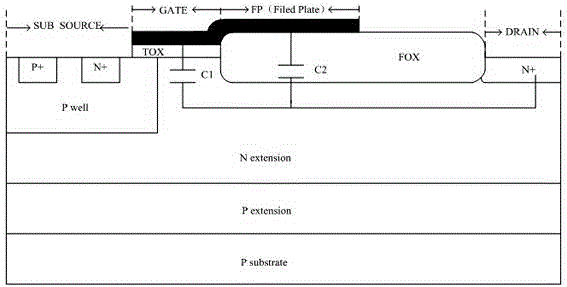
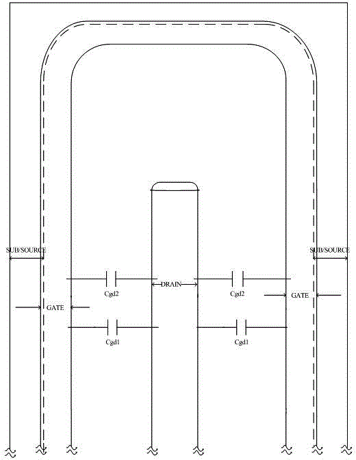
[0055] The cross-sectional schematic diagram of the cell structure of an LDMOS high-voltage device integrating independent high-voltage covering capacitors is shown in Figure 6 shown. Compared with the traditional LDMOS, the new structure is a five-terminal device with DRAIN, GATE, SOURCE, SUBSTRATE, and FP. Compared with traditional LDMOS, FP and GATE are disconnected to form both ends of LDMOS.

[0056] (1) The Cgd capacitor is composed of the GATE plate through the TOX (gate oxide layer) medium at the end of the channel, passing through the drift region and the drain (DRAIN) plate. Cgd is still in series with Cgs and Cgb, and is still affected by the Miller effect when applied.

[0057] (2) The CHV capacitor is formed between the FP plate passing through the FOX (field oxide layer) medium, passing through the drift region and the drain (DRAIN) plate. The FP field plate is POLY (polysilicon gate), and the drain (DRAIN) terminal is metal and semiconductor to form an ohmic...

Embodiment 2

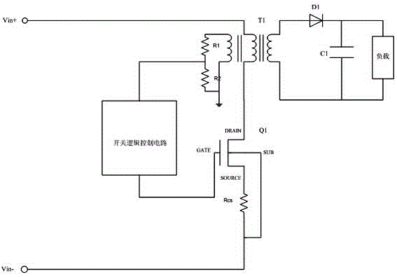
[0061] Embodiment 2 of the present invention proposes a circuit for demagnetization sampling using an HVMOS integrated demagnetization sampling device such as Figure 9 shown. The traditional demagnetization sampling circuit such as image 3 , Figure 4 shown. Traditional demagnetization sampling circuits require additional demagnetization sampling devices when detecting demagnetization. The demagnetization sampling circuit of the present invention includes an output rectifier circuit, a transformer T1, an integrated high-voltage capacitor LDMOS device Q1, a demagnetization signal sampling circuit 2, a demagnetization time timing circuit 3, and a switch logic control circuit 4.

[0062] One end of the primary of the transformer T1 is connected to the input Vin+, and the other end of the primary of the transformer T1 is connected to the drain (DRAIN) end of the switching device LDMOS. One end of the transformer T1 secondary is connected to the positive pole of the diode D1 ...


PUM


Abstract

The invention provides an HVMOS (high-voltage metal oxide semiconductor) integrated with a demagnetization sampling device, comprising a P substrate, an N drift region, an N-type doping drain end, a field oxide layer, a gate oxide layer, a P-type well source end, a field plate and a gate. The field plate and the drain end form a high-voltage covered capacitor through a medium therebetween. The independent high-voltage covered capacitor put forward in the invention is integrated in the HVMOS device without increasing the area of the HVMOS device. Moreover, the size of the high-voltage covered capacitor is adjustable, the use of the high-voltage capacitor is not influenced by series connection between a gate-source capacitor and a gate-substrate capacitor, the high-voltage capacitor is not connected in parallel with a traditional high-voltage drain-gate capacitor and is not affected by the Miller effect between the drain and the gate, and the high-voltage covered capacitor can be used as a demagnetization sampling device. The HVMOS area and the chip area are reduced.

Description

technical field [0001] The invention relates to the field of integrated circuit design, in particular to an HVMOS integrated demagnetization sampling device. Background technique [0002] In the design of the LED drive circuit, how to detect the end signal of the inductance demagnetization of the peripheral system in order to realize the constant current output of the system has become one of the keys to the current LED drive design. The method of sampling the demagnetization signal to the chip can be divided into two categories: 1. Use the resistor divider network around the chip to sample the demagnetization signal of the inductor and the primary coil of the transformer to the chip feedback port. 2. Use the demagnetization signal of the internal capacitor sampling system of the chip. The disadvantages of the first type of sampling technology are: (1), auxiliary windings and voltage divider resistors are required around the system, which increases the system cost; (2), the...

Claims


Application Information

Patent Timeline
IPC IPC(8): H01L29/78H01L29/423H01L21/336H01L21/28H05B37/02
Inventor 陈朝勇李育超
Owner CRM ICBG (WUXI) CO LTD
Features
  • R&D
  • Intellectual Property
  • Life Sciences
  • Materials
  • Tech Scout
  • Unparalleled Data Quality
  • Higher Quality Content
  • 60% Fewer Hallucinations
Learn More