Manufacturing method of light-emitting diode

A technology for light-emitting diodes and a manufacturing method, which is applied in the fields of semiconductor/solid-state device manufacturing, electrical components, and electrical solid-state devices, etc., can solve the problem of loss of reliability of high-voltage and high-power light-emitting diodes, reducing the life cycle of LED modules, and lengthy wire bonding and welding. Cost and other issues, to achieve the effect of reducing production cost, reducing resistance value and wire power consumption, and improving yield

Inactive Publication Date: 2016-06-15
杨秀静 +1
View PDF5 Cites 2 Cited by
  • Summary
  • Abstract
  • Description
  • Claims
  • Application Information

AI Technical Summary

Problems solved by technology

[0018] In the above-mentioned traditional method, because the light-emitting diode chip in the high-voltage and high-power light-emitting diode (LED) module can only dissipate heat through the very thin metal bonding wire and the sapphire base, the heat dissipation effect is poor, and the thermal stress caused by heat accumulation is extremely high. It is easy to disconnect the metal welding wire, which will lead to the loss of reliability of the high-voltage and high-power light-emitting diode (LED) module, and reduce the life cycle of the LED module; the traditional method of manufacturing LED modules is to separate the LED chips according to the design specifications with fine metal Wire welding to connect modules. The aforementioned grinding and thinning costs, cutting costs for laser separation of LED chips, poor heat dissipation after packaging, disconnection caused by thermal stress, lengthy and excessive wire bonding costs, and the reliability of LED modules Sex is a major bottleneck in the LED industry

Method used


Image

  • Manufacturing method of light-emitting diode
  • Manufacturing method of light-emitting diode
  • Manufacturing method of light-emitting diode

Examples


Embodiment

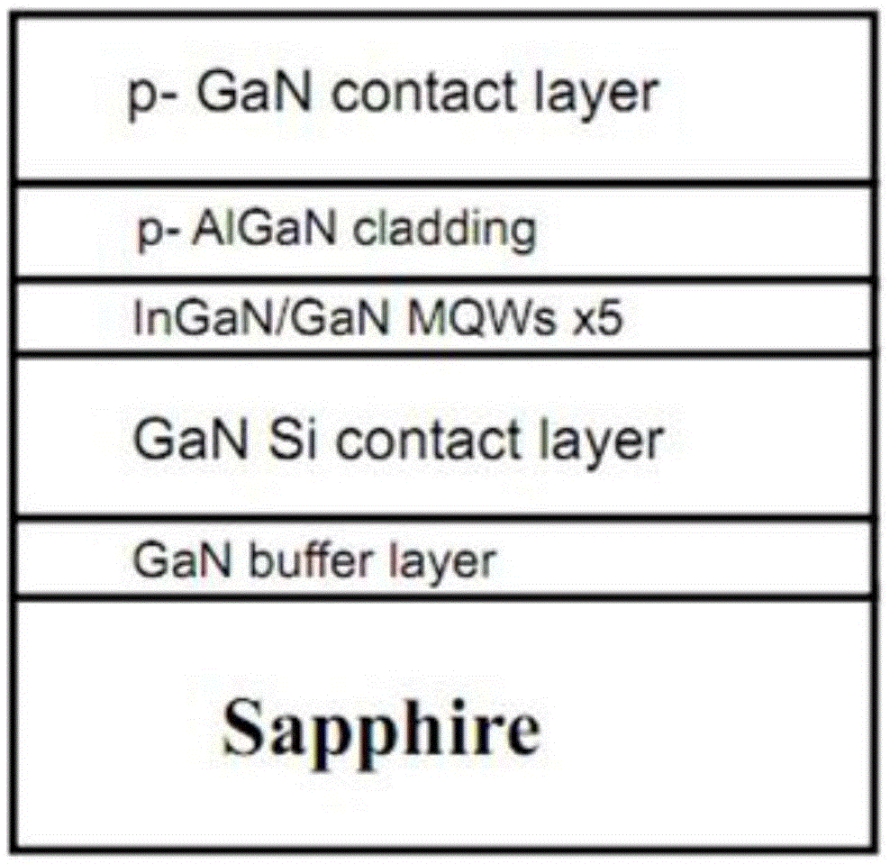
[0057] Example: A method for manufacturing light-emitting diodes disclosed in the present invention includes the following steps. Steps (1)-(7) are the same as the prior art. (1) ICP dry etching or laser cutting is used on the wafer Make a cutting channel on the sapphire crystal garden substrate to isolate each LED chip, such as image 3 Shown

[0058] (2) Growing 300nm thick SiO on the surface by PECVD 2 The thin film serves as a shielding layer for etching GaN, such as Figure 4 Shown

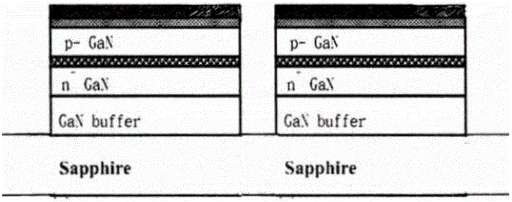
[0059] (3) Obtained by etching GaN with an ICP high-density plasma etching machine Figure 5 Mesa structure shown;

[0060] (4) Grow transparent electrodes Ni / Au on p-type GaN (e.g. Image 6 Shown);

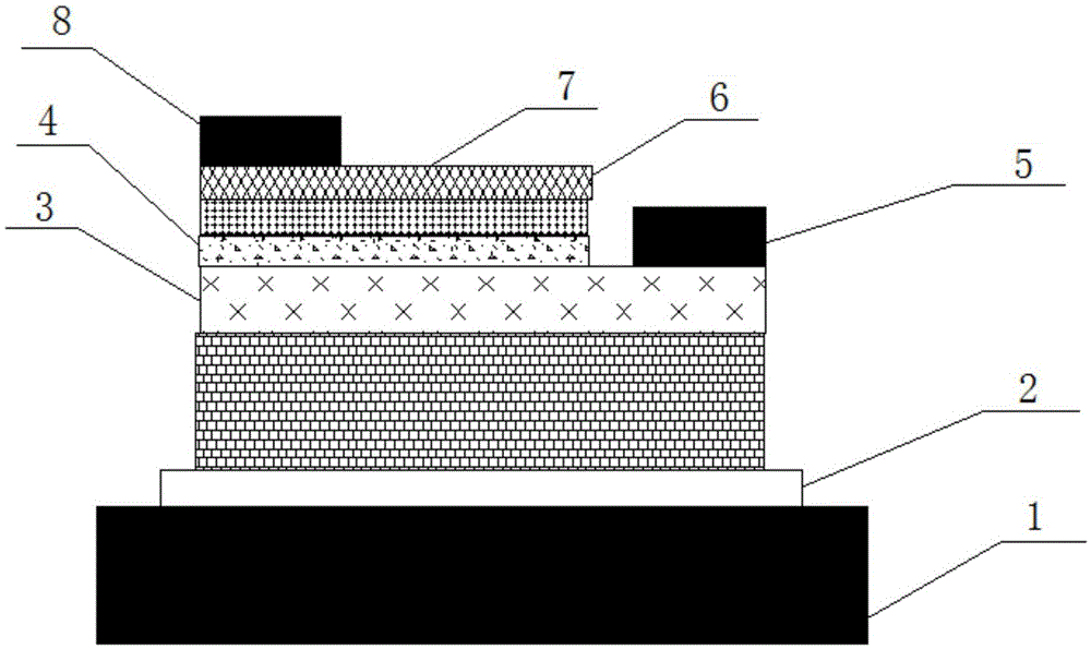
[0061] (5) Using lift-off process to simultaneously form ohm contacts and solder pads on Ni / Au transparent electrodes and n-type GaN, refer to the side structure of ohmic contacts and solder pads Figure 7 As shown, the front view of the pad area is as Figure 8 As shown, 13 indicates the pad position, ...


PUM


Abstract

The invention discloses a manufacturing method of a light-emitting diode. The light-emitting diode is manufactured by a metalized connection method. The method is characterized in that the sizes of modules are defined on a wafer; LED chips in the modules are firstly connected by a metalized connection technique for a semiconductor process; meanwhile, opening positions of welding pads are also defined; and the wafer is cut according to a cutting lane between the modules when cut, so that the cutting times is relatively few; and the production cost can be reduced. In addition, partial side walls of the LED chips are coated with metal layers; and these metal films (an aluminum bronze film, a gold film or a silver film) have excellent light reflectivity, so that photons irradiated to the side walls of the chips by LEDs are reflected to the surfaces of the LEDs to improve the luminous efficiency.

Description

Technical field [0001] The invention belongs to the technical field of lighting equipment, and specifically is a method for manufacturing a light emitting diode. Background technique [0002] Light-emitting diode, abbreviated as LED, is a kind of semiconductor electronic components that can convert electrical energy into light energy. Light-emitting diodes (LED) are usually made of sapphire substrate. The traditional LED chip structure is such as figure 1 As shown, 1-8 are metal base, adhesive material, n-type GaN, GaN quantum well, n-type electrode, p-type GaN, transparent electrode layer TCL, p-type electrode; the detailed structure of MOCVD epitaxial growth is sapphire substrate For the blue LED substrate, first grow a layer of GaN buffer layer of appropriate thickness, and then grow a layer of 3um thick n-type GaN contact layer doped with Si to grow InGaN / GaN multiple quantum well structure (at least 5-7 layers), and grow A very thin Mg-doped p-type AlGaN barrier layer (50nm)...

Claims


Application Information

Patent Timeline
Patent Type & Authority Applications(China)
IPC IPC(8): H01L33/00H01L33/60H01L33/62H01L33/64H01L21/304
CPCH01L2224/24137H01L33/007H01L21/3043H01L33/60H01L33/62H01L33/647H01L2933/0058H01L2933/0066H01L2933/0075
Inventor 杨秀静查国伟
Owner 杨秀静
Why Eureka
Try Eureka