A multilayer film with strong perpendicular magnetic anisotropy

An anisotropic, multi-layer film technology, used in the fields of non-volatile magnetic memory and magnetic logic, can solve the problem of not meeting the requirements of magnetic random access memory, insufficient thermal stability of the double interface structure, and increasing the number of thin film layers in the double interface structure, etc. problem, to achieve the effect of reducing the critical inversion current, strong perpendicular magnetic anisotropy and thermal stability, and small critical inversion current

Active Publication Date: 2019-03-15
致真存储(北京)科技有限公司
View PDF7 Cites 0 Cited by
  • Summary
  • Abstract
  • Description
  • Claims
  • Application Information

AI Technical Summary

Problems solved by technology

However, the double-interface structure increases the number of film layers, thus increasing the process complexity
Meanwhile, the thermal stability of dual-interface structures based on MgO / CoFeB / Ta / CoFeB / MgO is still insufficient
For example, when the cross-sectional diameter of the MgO / CoFeB / Ta / CoFeB / MgO structure is 11nm, the thermal stability factor is less than 30, which cannot meet the requirements of MRAM (Sato et al., Applied Physics Letters105, 062403(2014))

Method used


Image

  • A multilayer film with strong perpendicular magnetic anisotropy
  • A multilayer film with strong perpendicular magnetic anisotropy
  • A multilayer film with strong perpendicular magnetic anisotropy

Examples


Embodiment 1

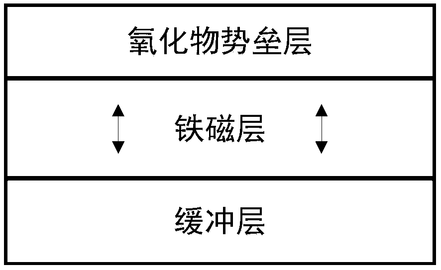
[0059] This embodiment is a specific example of solution one. In this embodiment, the buffer layer, the ferromagnetic layer and the oxide barrier layer are deposited on the thermally oxidized silicon substrate in order from bottom to top by magnetron sputtering, and the oxide barrier layer is deposited on the A protective layer such as Figure 4 shown. Finally, photolithography, etching and other processing are carried out, and the cross-sectional area is circular.

[0060] Among them, the buffer layer material is Bi with a thickness of 1nm; the ferromagnetic layer material is Co 20 Fe 60 B 20 , the thickness is 2.5nm; the oxide barrier layer material is MgO, the thickness is 1nm; the protective layer material is Ta, the thickness is 5nm. Because the Bi / CoFeB interface has a strong interfacial perpendicular magnetic anisotropy, when the CoFeB is 2.5nm, the interfacial perpendicular magnetic anisotropy is still sufficient to overcome the demagnetization field, so that the ...

Embodiment 2

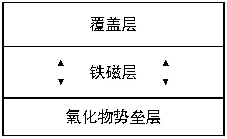
[0062] This embodiment is a specific example of the second solution. In this embodiment, the oxide barrier layer, the ferromagnetic layer and the cover layer are deposited on the thermally oxidized silicon substrate in order from bottom to top by magnetron sputtering, and a protective layer is deposited on the cover layer. layer, such as Figure 5 shown. Finally, photolithography, etching and other processing are carried out, and the cross-sectional area is circular.

[0063] Among them, the oxide barrier layer material is MgO, the thickness is 1nm; the ferromagnetic layer material is Co 20 Fe 60 B 20 , the thickness is 2.5nm; the cover layer material is Bi, the thickness is 1nm; the protection layer material is Ta, the thickness is 5nm. Because the CoFeB / Bi interface has a strong interfacial perpendicular magnetic anisotropy, when the CoFeB is 2.5nm, the interfacial perpendicular magnetic anisotropy is still sufficient to overcome the demagnetization field, so that the d...

Embodiment 3

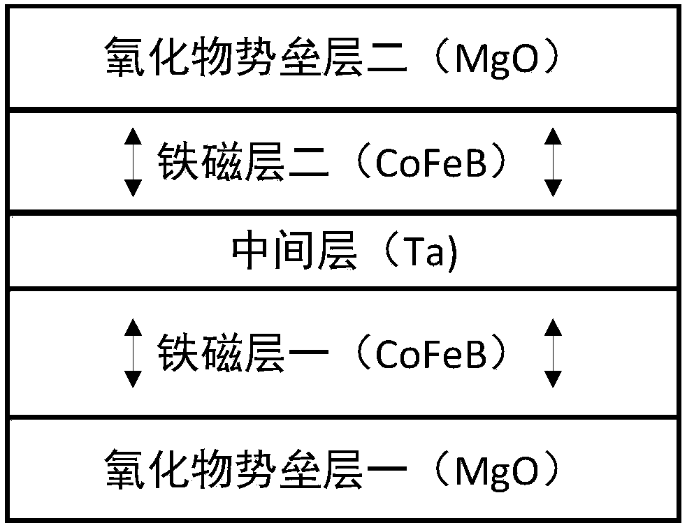
[0065] This embodiment is a specific example of the third solution. In this embodiment, oxide barrier layer 1, ferromagnetic layer 1, intermediate layer, ferromagnetic layer 2, and oxide barrier layer 2 are deposited on the thermal oxidation layer in order from bottom to top by magnetron sputtering. On the silicon substrate, and deposit a protective layer on the oxide barrier layer 2, such as Figure 6 shown. Finally, photolithography, etching and other processing are carried out, and the cross-sectional area is circular.

[0066] Among them, the material of the middle layer is Bi with a thickness of 0.4nm; the material of the ferromagnetic layer 1 is Co 20 Fe 60 B 20 , the thickness is 3nm; the material of ferromagnetic layer 2 is Co 20 Fe 60 B 20 , with a thickness of 1 nm; the oxide barrier layer 1 and the oxide barrier layer 2 are made of MgO with a thickness of 1 nm; the protective layer is made of Ta with a thickness of 5 nm. This is a double-interface structure ...


PUM

PropertyMeasurementUnit
thicknessaaaaaaaaaa
thicknessaaaaaaaaaa
thicknessaaaaaaaaaa

Abstract

The invention discloses a multilayer film with strong vertical magnetic anisotropy. The multilayer film with strong vertical magnetic anisotropy is characterized in that the strong vertical magnetic anisotropy is obtained by adopting strong interface vertical magnetic anisotropy of an interface between Bi or Bi alloy and a ferromagnetic layer. Four implementation schemes in total are provided in the invention. The scheme 1 is that the multilayer film structure comprises a buffer layer, a ferromagnetic layer and an oxide barrier layer sequentially from downside to upside. The scheme 2 is that the multilayer film structure comprises an oxide barrier layer, a ferromagnetic layer and a cover layer sequentially from downside to upside. The scheme 3 is that the multilayer film structure comprises a first oxide barrier layer, a first ferromagnetic layer, a middle layer, a second ferromagnetic layer and a second oxide barrier layer sequentially from downside to upside. A base also can be arranged below the first oxide barrier layer. The scheme 4 is that the multilayer film structure comprises a buffer layer, a first ferromagnetic layer, an oxide barrier layer, a second ferromagnetic layer and a cover layer sequentially from downside to upside. The multilayer film structure can serve as a core structure of a magnetic tunnel junction.

Description

【Technical field】 [0001] The invention relates to a multilayer film with strong perpendicular magnetic anisotropy, which belongs to the technical field of nonvolatile magnetic memory and magnetic logic. 【Background technique】 [0002] Magnetic random access memory (MRAM) has the advantages of non-volatility, unlimited erasing and writing, and fast read and write speeds. It is expected to become the next generation of low-power general-purpose memory, and has attracted extensive attention from industry and academia. . [0003] The core device of the MRAM is the magnetic tunnel junction (Magnetic Tunnel Junction, MTJ). The magnetic tunnel junction is mainly composed of three layers: a reference layer (Reference Layer), an oxide barrier layer (Barrier Layer), and a free layer (Free Layer). Wherein, the reference layer and the free layer are composed of ferromagnetic layer materials, and the oxide barrier layer is generally composed of metal oxides. The magnetization directio...

Claims


Application Information

Patent Timeline
Patent Type & Authority Patents(China)
IPC IPC(8): H01F10/32G11C11/15
CPCG11C11/161
Inventor 赵巍胜彭守仲张有光
Owner 致真存储(北京)科技有限公司
Why Eureka
Try Eureka