Enhanced-mode high electron mobility transistor, preparation method thereof, and semiconductor device

A high electron mobility, enhanced technology, applied in the direction of semiconductor devices, semiconductor/solid-state device manufacturing, electrical components, etc., can solve the problems of increasing device leakage and reducing device breakdown voltage, so as to improve breakdown voltage and reduce leakage , the effect of reducing surface damage

Inactive Publication Date: 2016-06-29
INST OF SEMICONDUCTORS - CHINESE ACAD OF SCI
View PDF3 Cites 49 Cited by
  • Summary
  • Abstract
  • Description
  • Claims
  • Application Information

AI Technical Summary

Problems solved by technology

However, due to the damage of the etching process, the leakage of the...

Method used


Image

  • Enhanced-mode high electron mobility transistor, preparation method thereof, and semiconductor device
  • Enhanced-mode high electron mobility transistor, preparation method thereof, and semiconductor device
  • Enhanced-mode high electron mobility transistor, preparation method thereof, and semiconductor device

Examples


preparation example Construction

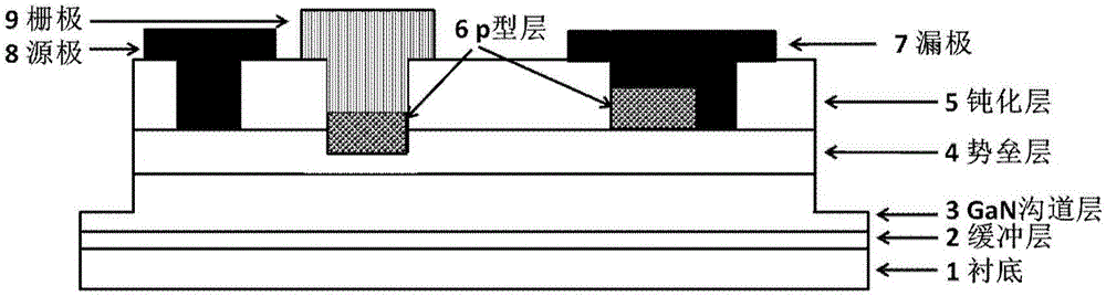
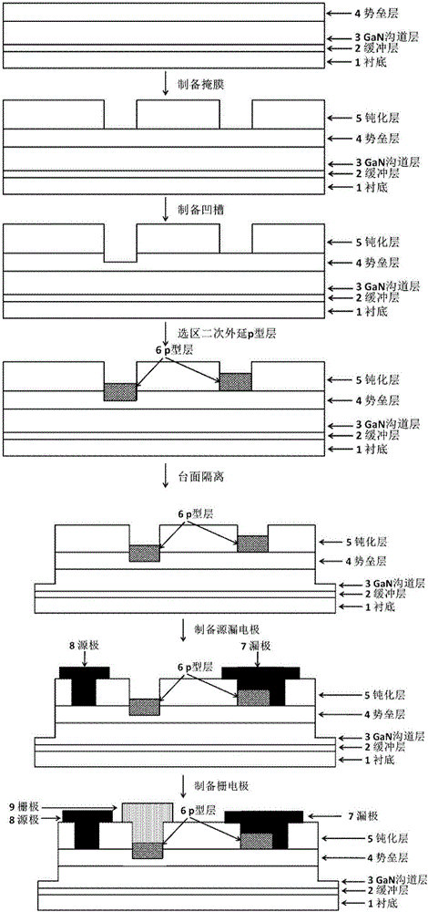
[0046] Based on the same inventive concept, the present invention provides a method for preparing an enhanced high electron mobility transistor, comprising the following steps:

[0047] S1: Prepare an epitaxial layer on the substrate, including preparing a barrier layer;

[0048] S2: depositing a passivation layer on the barrier layer;

[0049] S3: Preparing a secondary epitaxial mask for selected areas;
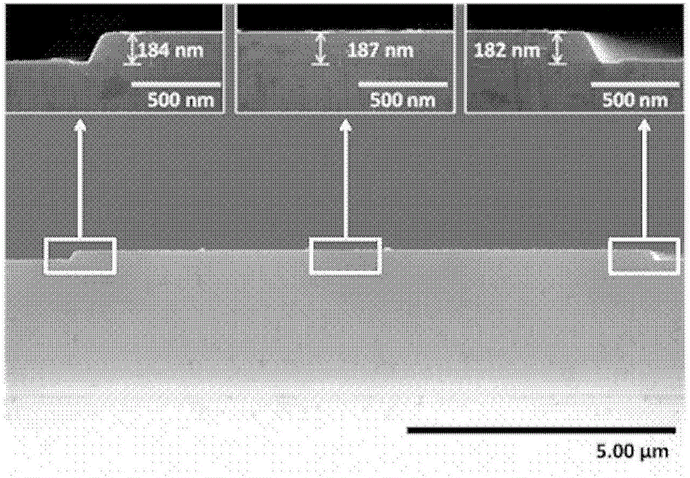
[0050] S4: In the local area of ​​the secondary epitaxial mask of the selected area, etch down from the barrier layer to prepare grooves;

[0051] S5: growing a p-type layer on the selective secondary epitaxial mask region and the groove;

[0052] S6: Prepare the source and drain electrodes, wherein the drain electrode is in contact with the p-type layer metal grown on the non-groove;

[0053] S7: preparing a gate electrode on the surface of the p-type layer grown in the groove.

[0054] Preferably, the doping concentration of the p-type layer is 1×10 16 -1×10 22 cm -3 ...


PUM

PropertyMeasurementUnit
Etching depthaaaaaaaaaa
Thicknessaaaaaaaaaa
Thicknessaaaaaaaaaa

Abstract

The present invention provides an enhanced-mode high electron mobility transistor. The transistor includes a grid electrode, a source electrode, a drain electrode, a p type layer, a barrier layer, and a passivation layer arranged on the barrier layer. A part region on the passivation layer is provided with a secondary epitaxy figure formed by etching to the upper surface of the barrier layer. The barrier layer also includes a trench formed by further etching to the inner side of the barrier layer in a local region of the figure. The p type layer that is grown through secondary epitaxy is in the figure and the trench. The p type layer in the trench is contacted with a grid electrode metal on the p type layer in the trench. The p type layer that is not in the trench is contacted with a drain electrode metal on the p type layer that is not in the trench. The present invention also provides a preparation method of the transistor and a semiconductor device including the transistor. According to the transistor, due to a trench grid and the p type layer grown through secondary epitaxy in a selected region, a threshold voltage of the device is increased; and a part of the barrier layer is etched, so that a saturated current of the device is greater than the current of the trench grid type high electron mobility transistor (HEMT). In addition, the p type layer is also grown in a selected region of the drain electrode metal, so that the turn-off effect of the device is improved.

Description

technical field [0001] The invention belongs to the technical field of semiconductors, in particular to an enhanced high electron mobility transistor, a preparation method thereof, and a semiconductor device including the transistor. Background technique [0002] GaN-based power electronic devices have attracted a lot of attention in recent years. GaN materials can form heterojunction structures with AlGaN, InAlN and other materials. Due to the spontaneous polarization and piezoelectric polarization effects of the barrier layer materials, a high concentration of two-dimensional electron gas (2DEG) will be formed at the heterojunction interface. [0003] GaN-based HEMT (High Electron Mobility Transistor) devices are widely used in power electronics fields such as electric vehicles, wind power generation, and power management due to their high saturation current, high breakdown voltage, and fast switching speed. Yole Development estimates that the most suitable voltage range...

Claims


Application Information

Patent Timeline
IPC IPC(8): H01L29/778H01L21/335
CPCH01L29/7786H01L29/66462
Inventor 黄宇亮程哲张连张韵王军喜李晋闽
Owner INST OF SEMICONDUCTORS - CHINESE ACAD OF SCI
Why Eureka
Try Eureka