Ceramic substrate planarization manufacturing method

A production method and ceramic substrate technology, applied in the field of ceramic substrate production, can solve the problems of poor uniformity of substrate coating edges, adverse effects on the health of production personnel, poor coating uniformity, etc., and achieve controllable glaze layer thickness and fluidity Good, improve flatness effect

Inactive Publication Date: 2016-07-13
UNIV OF ELECTRONICS SCI & TECH OF CHINA
View PDF4 Cites 3 Cited by
  • Summary
  • Abstract
  • Description
  • Claims
  • Application Information

AI Technical Summary

Problems solved by technology

However, the sol-gel method has a series of unavoidable disadvantages: the tetraethyl orthosilicate used in the above-mentioned patent is narcotic, irritating, and has certain toxicity at high concentrations, which adversely affects the health of production personnel; The coating method of sol-spin coating will lead to poor uniformity of the coating edge of the substrate, and the uniformity of the entire coating will also become poor after multiple coatings, which can only be applied to the small-scale ordinaryization of the substrate. Therefore, the above-mentioned technology is not suitable for large-area planarization of substrates.

Method used


Image

  • Ceramic substrate planarization manufacturing method
  • Ceramic substrate planarization manufacturing method
  • Ceramic substrate planarization manufacturing method

Examples


Embodiment 1

[0023] (1) the mass percent SiO 2 41%, Al 2 o 3 13%, CaO17%, MgO4%, BaO10%, Na 2 O8% and K 2 O7% mixed evenly, ball milled for 24 hours.

[0024] (2) Dried in an oven, melted in a high-temperature electric furnace at 1390 degrees to a clear state, kept at the highest temperature for 15 minutes, and then quenched with deionized water.

[0025] (3) Grind the quenched glass clinker to the size of salt particles, and then ball mill for 72 hours.

[0026] (4) Sieve through a 300-mesh sieve, and then mix with the organic carrier at a mass percentage of 1:1. The organic carrier consists of 110ml terpineol, 2g hydrogenated castor oil, 8g ethyl cellulose, and 30ml dimethyl phthalate and 2g of Tween 80 were uniformly mixed, and stirred in an 85°C water bath atmosphere for 8 hours to form a slurry.

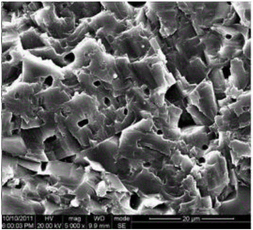
[0027] (5) Using the screen printing method, a 300-mesh screen plate was used to print three times on the surface of the substrate to obtain a glaze with a thickness of 60 um, and sint...

Embodiment 2

[0029] (1) the mass percent SiO 2 62%, Al 2 o 3 13%, CaO11%, MgO4%, BaO4%, Na 2 O2% and K 2 O4% mixed evenly, ball milled for 24 hours.

[0030] (2) Dried in an oven, melted in a high-temperature electric furnace at 1450°C to a clear state, kept at the highest temperature for 30 minutes, and then quenched with deionized water.

[0031] (3) Grind the quenched glass clinker to the size of salt particles, and then ball mill for 72 hours.

[0032] (4) Sieve through a 300-mesh sieve, and then mix with the organic carrier at a mass percentage of 1:1. The organic carrier consists of 110ml terpineol, 2g hydrogenated castor oil, 8g ethyl cellulose, and 30ml dimethyl phthalate Esters and 2g of Tween 80 were evenly mixed, and stirred in an 85°C water bath atmosphere for 8 hours to make a slurry.

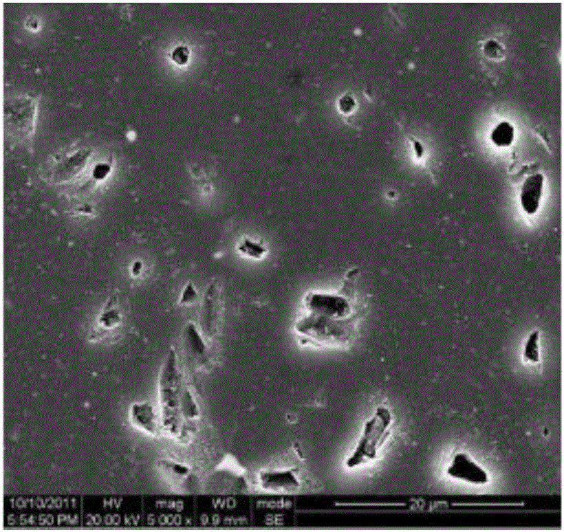
[0033] (5) Using the screen printing method, a 300-mesh screen plate was used to print three times on the surface of the substrate to obtain a glaze with a thickness of 60 um, and sintere...


PUM

PropertyMeasurementUnit
surface roughnessaaaaaaaaaa

Abstract

The invention belongs to the technical field of ceramic substrate production, and in particular relates to a ceramic substrate planarization manufacturing method for a film circuit. High-temperature glaze matched with the ceramic substrate is applied to the field of the film circuit substrate planarization. The ceramic substrate planarization manufacturing method is characterized in that a thin high-temperature glass glaze layer which has a thermal expansion coefficient similar with that of a substrate is coated on the surface of the substrate. The glass glaze takes following Ca / Al / Si-series glass in percentage by mass as the main components: 41-65% of SiO2, 9-13% of Al2O3, 10-17% of CaO, additives comprising 1-4% of MgO, 4-10% of BaO, 1-9% of Na2O, and 1-9% of K2O. A planarization substrate product manufactured by the ceramic substrate planarization manufacturing method does not have cracks on surface, does not generate wrinkles, has surface roughness Ra of 0.2 nm-0.5 nm within a range of 20*20 mum<2>, has surface roughness Ra of 0.5 nm-0.62 nm within a range of 100*100 mum<2>, and has surface roughness Ra of 0. 5nm-31.68 nm within a range of 2000*2000 mum<2>.

Description

technical field [0001] The invention belongs to the technical field of ceramic substrate production, and in particular relates to a method for planarizing and modifying a ceramic substrate for thin film circuits. Background technique [0002] Ceramic substrates are widely used in the field of microwave devices because of their good microwave properties. However, the roughness of the surface of the ceramic substrate seriously affects the performance of the microwave circuit fabricated on the substrate, and hinders the development of the microwave circuit towards the direction of miniaturization and integration. Taking the beryllium oxide ceramic substrate as an example, the surface of the polished substrate is smoother than that of the unpolished substrate. However, the cost of polishing is too high, and there are some unpredictable holes on the surface, which will still affect the performance and integration of microwave circuits. degree of influence. [0003] Chinese pate...

Claims


Application Information

Patent Timeline
Patent Type & Authority Applications(China)
IPC IPC(8): C04B41/86C03C8/16
CPCC04B41/86C03C8/16C04B41/5022C04B41/4539
Inventor 张继华石玉龙杨传仁陈宏伟
Owner UNIV OF ELECTRONICS SCI & TECH OF CHINA
Why Eureka
Try Eureka