An on-chip integrated polarization beam splitter and its polarization beam splitting method

A polarization beam splitter and integrated technology, applied in the field of integrated optics, can solve the problems of large waveguide size, low optical signal mode field limitation, low refractive index, etc., and achieve large working bandwidth, compact structure, and large device manufacturing tolerance Effect

Active Publication Date: 2019-09-03
SOUTHEAST UNIV
View PDF6 Cites 0 Cited by
  • Summary
  • Abstract
  • Description
  • Claims
  • Application Information

AI Technical Summary

Problems solved by technology

However, due to its low refractive index (about 2.0), the limitation of the optical signal mode field is low, resulting in the need for a larger waveguide size to carry the optical signal mode

Method used


Image

  • An on-chip integrated polarization beam splitter and its polarization beam splitting method
  • An on-chip integrated polarization beam splitter and its polarization beam splitting method
  • An on-chip integrated polarization beam splitter and its polarization beam splitting method

Examples


Embodiment 1

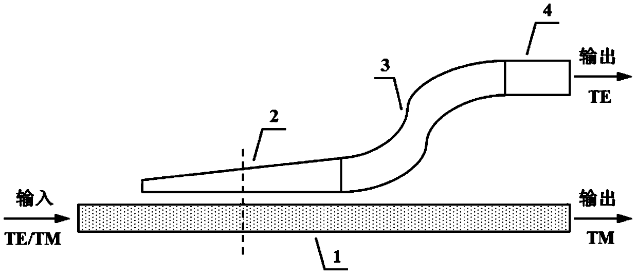
[0033] Embodiment 1: as Figure 1 to Figure 2 Shown is the structural diagram of the first embodiment of the present invention, and it comprises:

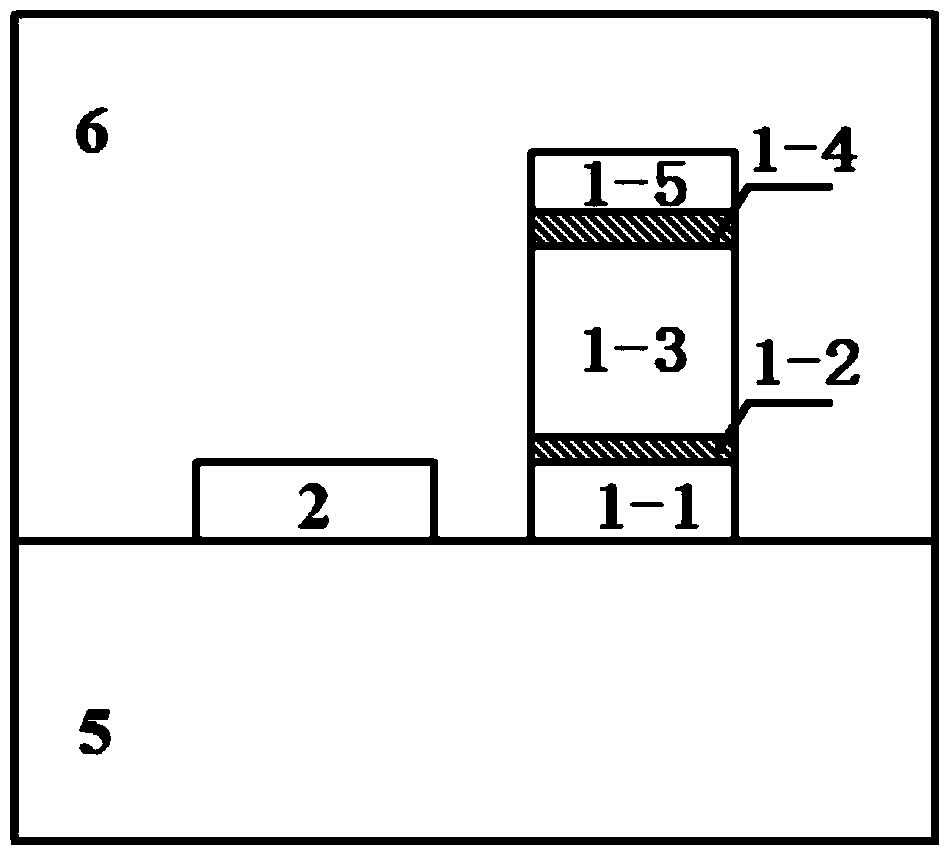
[0034]The substrate 5 is provided with a hybrid plasmonic waveguide 1, a taper-type coupling waveguide, an S-curve waveguide 3, and an output silicon waveguide 4 of the same thickness; a taper-type coupling waveguide, an S-curve waveguide 3, and an output silicon waveguide 4 in sequence In series and located on the same side of the hybrid plasmonic waveguide 1, the taper-type coupling waveguide and the hybrid plasmonic waveguide 1 are arranged in parallel; the hybrid plasmonic waveguide 1 is divided into metal covering layers 1-5, upper silicon dioxide layers 1-4, nitrogen Silicone waveguide layer 1-3, lower silicon dioxide layer 1-2 and silicon waveguide layer 1-1; coupling waveguide 2, S-curve waveguide 3 and output silicon waveguide 4 have the same thickness as silicon waveguide layer 1-1 ; The coupling waveguide 2 is a silicon...

Embodiment 2

[0039] Example 2: Figure 8 As the second embodiment of the present invention, an improved multimode interference coupler is used instead of a taper type directional coupler to couple the TE mode out. The multimode interference coupler is a rectangular waveguide. In order to reduce the reflection loss of the multimode interference coupler, we truncate the corner away from the hybrid plasmonic waveguide 1 among the two corners of the input end of the multimode interference coupler, which can effectively reduce the input and The influence of the partial reflection loss caused by the structural size mismatch between the output waveguide and the multimode interference coupler on the transmission performance. By optimizing the width and longitudinal transmission length of the multimode interference coupler, two high-performance linearly polarized modes, TE and TM, can be obtained at the output.

Embodiment 3

[0040] Example 3: Figure 9 The third embodiment of the present invention includes: a substrate 5, a hybrid plasmon waveguide 1 is arranged on the substrate 5, and a first coupling waveguide 2-1 and a second coupling waveguide 2-1 are respectively arranged on both sides of the hybrid plasmon waveguide 1. 2. The distance between the first coupling waveguide 2-1 and the second coupling waveguide 2-2 is equal to the hybrid plasmonic waveguide 1; the output end of the first coupling waveguide 2-1 is connected to the first output end through the first S-bend waveguide 3-1 The silicon waveguide 4-1 is connected; the output end of the second coupling waveguide 2-2 is connected with the second output silicon waveguide 4-2 through the second S-bend waveguide 3-2; the hybrid plasmonic waveguide 1 is divided into metal covering from top to bottom layer 1-5, upper silicon dioxide layer 1-4, silicon nitride waveguide layer 1-3, lower silicon dioxide layer 1-2 and silicon waveguide layer 1-...


PUM


Abstract

The invention provides an on-chip integrated polarization beam splitter and a polarization beam splitting method thereof. The on-chip integrated polarization beam splitter comprises a hybrid plasma waveguide, a coupling waveguide, an S-bend waveguide and an output silicon waveguide, wherein the coupling waveguide, the S-bend waveguide and the output silicon waveguide are located on the same side of the hybrid plasma waveguide, are sequentially connected in series and are equal in thickness. The hybrid plasma waveguide is divided into a metal coverage layer, an upper silicon dioxide layer, a silicon nitride waveguide layer, a lower silicon dioxide layer and a silicon waveguide layer from top to bottom. The coupling waveguide, the S-bend waveguide and the output silicon waveguide are equal to the silicon waveguide layer in thickness. The coupling waveguide is a silicon waveguide. After input signals including transverse electric modes and transverse magnetic modes enter a coupling zone, transverse electric mode light signals are coupled to the taper-type coupling waveguide and then are output through the S-bend waveguide and the output silicon waveguide, and the transverse magnetic mode light signals are directly transmitted along the hybrid plasma waveguide and are directly output, and waveguide coupling does not occur. The on-chip integrated polarization beam splitter has the advantages of being small in size, compact in structure, high in polarization extinction ratio, low in insertion loss, larger in working bandwidth and the like.

Description

technical field [0001] The invention relates to the technical field of integrated optics, in particular to an on-chip integrated polarization beam splitter and a polarization beam splitting method thereof. Background technique [0002] In recent years, photonic integrated circuit technology has received extensive attention from researchers, and the most important material platform is silicon-on-insulator (SOI) based on high refractive index difference waveguide structure. However, the structure with high refractive index difference will bring strong polarization sensitivity to the device and system, especially when the optical signal is coupled from the optical fiber to the waveguide chip, since the polarization state in the optical fiber changes randomly, the polarization problem will be changed. is particularly prominent. At present, on-chip polarization diversity schemes are mainly used to solve the polarization sensitivity problem of high refractive index difference wav...

Claims


Application Information

Patent Timeline
Patent Type & Authority Patents(China)
IPC IPC(8): G02B6/126G02B6/122
Inventor 肖金标徐银
Owner SOUTHEAST UNIV
Why Eureka
Try Eureka