Pd/MoS2/SiO2/Si/SiO2/In multi-junction photo-detector and preparation method thereof

A light detection and device technology, applied in semiconductor devices, electrical components, final product manufacturing, etc., can solve the problems of not having self-driven light response function and light detection performance, and can not be applied to the field of infrared light detection, etc., to achieve fast binary light response , reduce the reverse dark current, increase the effect of photogenerated current

Inactive Publication Date: 2016-07-13
CHINA UNIV OF PETROLEUM (EAST CHINA)
View PDF3 Cites 3 Cited by
  • Summary
  • Abstract
  • Description
  • Claims
  • Application Information

AI Technical Summary

Problems solved by technology

[0010] However, the above two solar cell devices do not have good self-driven photoresponse funct

Method used


Image

  • Pd/MoS2/SiO2/Si/SiO2/In multi-junction photo-detector and preparation method thereof
  • Pd/MoS2/SiO2/Si/SiO2/In multi-junction photo-detector and preparation method thereof
  • Pd/MoS2/SiO2/Si/SiO2/In multi-junction photo-detector and preparation method thereof

Examples


Embodiment 1

[0074] The preparation method is as follows:

[0075] (1) Select an n-type Si single crystal substrate with a resistivity of 1-10Ω cm;

[0076] (2) pre-treat the selected Si single crystal substrate: ultrasonic cleaning in alcohol, acetone and deionized water for 180 s, and then ultrasonic cleaning in a hydrofluoric acid solution with a concentration of 4% by volume for 60 s, after taking it out, Sweep with nitrogen to dryness;

[0077] (3) Put the Si single crystal substrate from which the intrinsic oxide layer has been removed into a beaker filled with a 30% hydrogen peroxide solution, put the beaker into a water bath, and heat it in a water bath at 95°C for 20 minutes passivation of silicon surfaces;

[0078] (4) Put the Si single crystal substrate after passivating the surface into deionized water to clean for one minute, after taking it out, dry it with high-purity nitrogen;

[0079] (5) Put the passivated Si substrate into the tray and put it into the vacuum chamber, ...

Embodiment 2

[0085] In Example 1, 4% hydrofluoric acid was ultrasonically cleaned for 20 seconds, and the Si single crystal substrate was passivated with 30% hydrogen peroxide for 5 minutes at 20° C.;

[0086] All the other are the same as in Example 1.

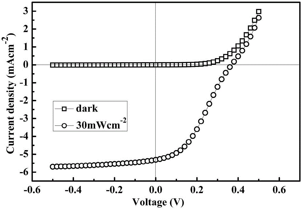
[0087] After testing, the prepared Pd / SiO 2 / Si / SiO 2 / In multi-junction photodetection devices at 1μW / cm 2 Under the light conditions, the open circuit voltage is 10mV and the short circuit current is 80nA. Based on the photovoltaic characteristics, when the wavelength is 400nm, the response rate is 0.15A / W, when the wavelength is 500nm, the response rate is 0.3A / W, and the wavelength is 920nm , the responsivity is 0.6A / W, and when a small forward bias voltage is applied to the device, it has a binary photoresponse function.

Embodiment 3

[0089] In Example 1, 4% hydrofluoric acid was ultrasonically cleaned for 90 seconds, and the Si single crystal substrate was passivated with 30% hydrogen peroxide for 60 minutes at 100° C.;

[0090] All the other are the same as in Example 1.


PUM

PropertyMeasurementUnit
Thicknessaaaaaaaaaa
Thicknessaaaaaaaaaa
Thicknessaaaaaaaaaa

Abstract

The invention discloses a Pd/MoS2/SiO2/Si/SiO2/In multi-junction photo-detector and a preparation method thereof. The Pd/MoS2/SiO2/Si/SiO2/In multi-junction photo-detector has a self-driving function, under irradiation of white light of 30mWcm<-2>, the density of optical excitation currents generated by the device reaches 5.3mAcm<-2>; under a monochromatic light condition of quite weak light intensity (1.0[mu]Wcm<-2>), the photo-detector still demonstrate photoresponse performance far higher than other devices of the same type; and when quite small bias positive voltages are applied to the device, under a pulse-type illumination condition, the direction of output currents can be rapidly alternatively changed from positive to negative, such that rapid binary-system photoresponse can be realized, and the detection precision of weak infrared optical signals is substantially improved. The photoresponse device provided by the invention has the advantages of rapid response speed, short recovery time, good periodicity, simple preparation technology, high yield and the like, thereby being suitable for large-scale industrial production.

Description

technical field [0001] The present invention relates to a photodetection device based on a semiconductor heterojunction and a preparation method thereof, in particular to a palladium / molybdenum disulfide / silicon dioxide / silicon / silicon dioxide / indium multi-junction photodetection device and a preparation method thereof, It belongs to the field of semiconductor devices. Background technique [0002] In recent years, the development of self-driven photodetection devices has attracted extensive attention from many researchers at home and abroad. The main reason is that compared with traditional photodetection devices, self-driven photodetection devices do not require any external bias power supply during operation. . This will significantly reduce the power consumption of the device, and at the same time greatly simplify the circuit of the device and increase the integration of device functions. [0003] In the prior art, various self-driven photodetection devices generally h...

Claims


Application Information

Patent Timeline
IPC IPC(8): H01L31/11H01L31/18
CPCH01L31/11H01L31/18Y02P70/50
Inventor 郝兰众高伟刘云杰韩治德薛庆忠
Owner CHINA UNIV OF PETROLEUM (EAST CHINA)
Why Eureka
Try Eureka