Schottky barrier semiconductor rectifier and manufacturing method therefor

A Schottky potential and rectifier technology, applied in semiconductor/solid-state device manufacturing, semiconductor devices, electrical components, etc., can solve problems such as increasing the series resistance of the conductive channel, low doping concentration of the epitaxial layer, and forward voltage drop. , to achieve the effect of increasing the density of the conductive channel, reducing the series resistance, and reducing the forward voltage drop.

Active Publication Date: 2016-07-20
HANGZHOU LION MICROELECTRONICS CO LTD
View PDF9 Cites 14 Cited by
  • Summary
  • Abstract
  • Description
  • Claims
  • Application Information

AI Technical Summary

Problems solved by technology

However, due to the limitations of the methods for forming short channels and channel doping gradient distribution, such devices are usually based on a planar gate structure, and there are junction field effect transistors formed by parasitic body doping regions inside the device, and the parasitic junction field effect transistors increase The series resistance on the conductive channel is increased, and at the same time, the increase of the conductive channel density is limited; in order to avoid the possible punch-through leakage caused by the short channel when the device is reverse biased, the doping concentration of the epitaxial layer is usually low, which further increases the Series resistance on the conduction channel; the above two points make the forward conduction voltage drop of the device at high current higher, usually higher than that of trench Schottky barrier diode
[0005] It can be seen that the prior art still has deficiencies in the forward conduction voltage drop of semiconductor rectifiers, and it is of great significance to further improve the device structure and manufacturing method

Method used


Image

  • Schottky barrier semiconductor rectifier and manufacturing method therefor
  • Schottky barrier semiconductor rectifier and manufacturing method therefor
  • Schottky barrier semiconductor rectifier and manufacturing method therefor

Examples


Embodiment Construction

[0059] The present invention will be further described below in conjunction with the accompanying drawings and specific embodiments.

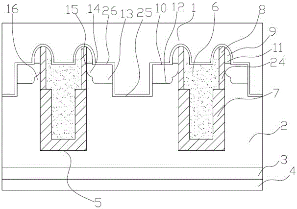
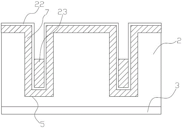
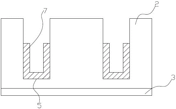
[0060] Such as figure 1 A Schottky barrier semiconductor rectifier shown includes an anode metal layer 1, a Schottky barrier metal layer 26, a lightly doped epitaxial layer 2 of the first conductivity type, and a heavily doped first conductivity type from top to bottom. A heterogeneous monocrystalline silicon substrate 3 and a cathode metal layer 4. A plurality of first grooves 5 are arranged laterally at intervals on the upper part of the epitaxial layer. The first grooves are filled with conductive polysilicon 6. There is a gap between the conductive polysilicon and the first grooves. The isolation layer 7 is provided with a silicon dioxide gate oxide layer 24, the thickness of the silicon dioxide gate oxide layer is smaller than that of the isolation layer, and the top of the silicon dioxide gate oxide layer extends upward and is higher than...


PUM


Abstract

The invention discloses a schottky barrier semiconductor rectifier. The schottky barrier semiconductor rectifier comprises a schottky barrier metal layer, an epitaxial layer and a first trench, wherein an isolating layer and a silicon dioxide gate-oxide layer are arranged in the first trench; the silicon dioxide gate-oxide layer extends upwards to form a dielectric wall; conductive polysilicon side walls are arranged on the two sides of the dielectric wall; a second trench is formed between the upper part of the epitaxial layer and the conductive polysilicon side walls; a transverse uniform doping region and a gradient doping region are arranged at the upper part of the epitaxial layer; a channel is formed between the gradient doping region and the silicon dioxide gate-oxide layer; spacer regions are arranged among the lower part of the epitaxial layer, the transverse uniform doping region, the gradient doping region and the silicon dioxide gate-oxide layer; a third trench is formed in the second trench; and the schottky barrier metal layer is positioned on the inner side surface of the third trench, and in contact with the epitaxial layer to form the schottky barrier. The schottky barrier semiconductor rectifier has good forward conduction characteristic and high device reliability. The invention also discloses a manufacturing method for the schottky barrier semiconductor rectifier; and the manufacturing method is large in process window, easy to control, low in photoetching number of times, and low in manufacturing cost.

Description

technical field [0001] The invention relates to the technical field of semiconductor device manufacturing, in particular to a Schottky barrier semiconductor rectifier and a manufacturing method thereof. Background technique [0002] As a conversion device of electric energy, semiconductor rectifiers have higher and higher requirements for performance improvement such as reducing forward voltage drop, increasing reverse blocking voltage, reducing reverse leakage, and increasing switching speed for the sake of improving system efficiency. . [0003] The PN junction diode used as a semiconductor rectifier earlier, due to the need to overcome the PN junction barrier during forward conduction, resulting in high forward conduction voltage drop, and the low switching speed caused by minority carrier injection during forward conduction, has been adopted by SCHOTT in many application fields. base barrier diodes instead. Schottky barrier diodes are usually composed of an N-type epit...

Claims


Application Information

Patent Timeline
Patent Type & Authority Applications(China)
IPC IPC(8): H01L29/872H01L21/329
CPCH01L29/66143H01L29/8725
Inventor 刘伟
Owner HANGZHOU LION MICROELECTRONICS CO LTD
Why Eureka
Try Eureka