Perovskite LED taking ZnO nanometer wall network as electron injecting layer and preparation method thereof

A technology of electron injection layer and nano wall, which is applied in the direction of circuits, electrical components, semiconductor devices, etc., can solve the problems of increasing the probability of non-radiative recombination of carriers, the decrease of device luminous efficiency, and poor film formation, so as to promote high efficiency The effect of radiative recombination

Active Publication Date: 2016-07-20
ZHENGZHOU UNIV
View PDF4 Cites 8 Cited by
  • Summary
  • Abstract
  • Description
  • Claims
  • Application Information

AI Technical Summary

Problems solved by technology

If the film-forming property of the perovskite layer is poor, its low surface coverage will inevitably lead to the generation of device leakage current, which will increase the probability of non-radiative recombination of carriers and reduce the luminous efficiency of the device.

Method used


Image

  • Perovskite LED taking ZnO nanometer wall network as electron injecting layer and preparation method thereof
  • Perovskite LED taking ZnO nanometer wall network as electron injecting layer and preparation method thereof
  • Perovskite LED taking ZnO nanometer wall network as electron injecting layer and preparation method thereof

Examples


preparation example Construction

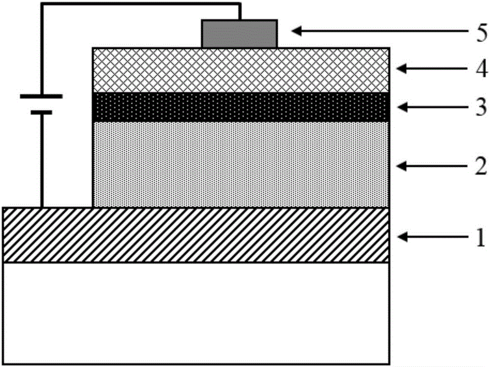
[0037] A preparation method of a perovskite LED using a ZnO nanowall network as an electron injection layer, the steps are as follows:

[0038] (1) cleaning the transparent conductive substrate 1;

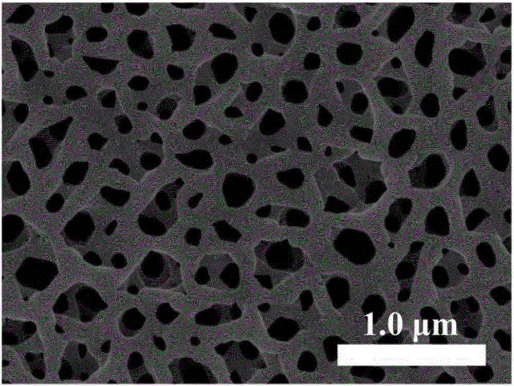
[0039] (2) Epitaxial growth of n-type ZnO nanowall network 2 on substrate 1 by MOCVD method;

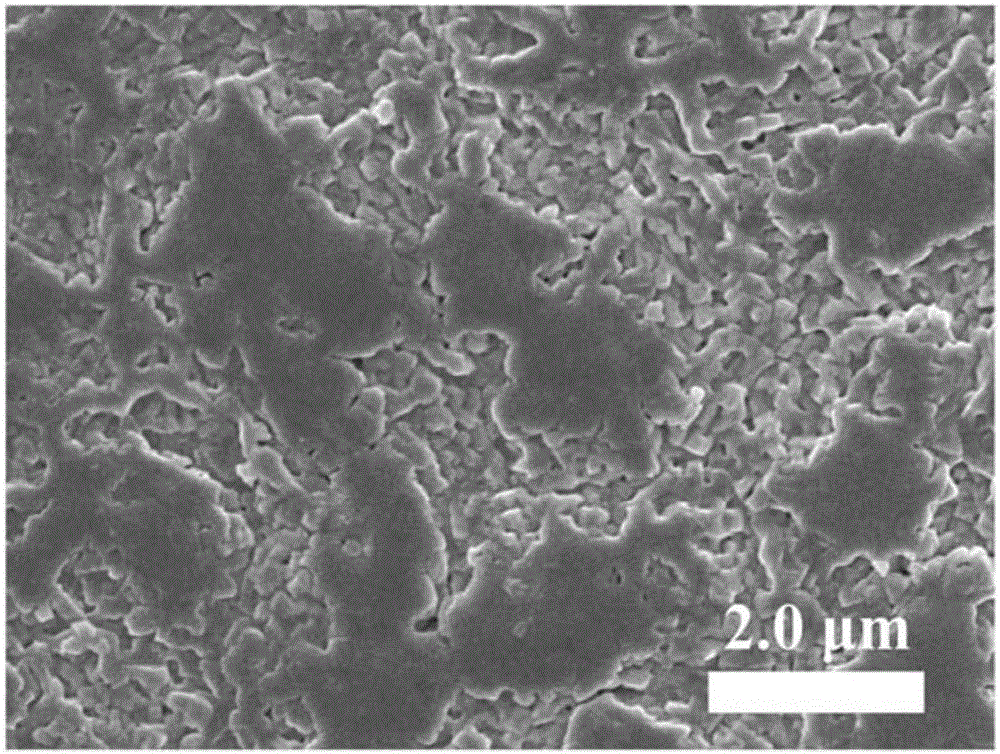
[0040] (3) Preparation of CH on n-type ZnO nanowall network 2 by low-temperature solution method 3 NH 3 PbBr 3 Light-emitting layer 3;

[0041] (4) in CH 3 NH 3 PbBr 3 Prepare a p-type hole-providing layer 4 on the light-emitting layer 3;

[0042] (5) A circular translucent electrode 5 is prepared on the p-type hole-providing layer 4 by thermal evaporation.

[0043] Preferably, the MOCVD preparation of the n-type ZnO nanowall network 2 in step (2) adopts a two-step growth method.

[0044] Step (3) CH 3 NH 3 PbBr 3 The preparation of the light-emitting layer 3 is a one-step low-temperature solution method or a two-step low-temperature solution method.

[0045] In step (4), the p...

Embodiment 1

[0048] 1) Use commercially available transparent and conductive ITO glass as the substrate 1, cut it into a required 20mm×20mm square, and then perform chemical cleaning on it. The specific cleaning steps are:

[0049] First, wash the substrate in detergent (Liby brand liquid detergent) for 15 minutes, then rinse it with tap water; then use acetone and ethanol solutions to ultrasonically clean it for 10 minutes each, and recirculate once; then rinse it with deionized water After cleaning, dry it with high-purity nitrogen before use.

[0050] 2) Put the cleaned ITO glass on the graphite tray in the MOCVD (vapor phase deposition) reaction chamber, and grow a two-dimensional n-type ZnO nanowall network 2 as the electron injection layer of the LED by a two-step growth method. The specific growth conditions are as follows:

[0051] In the first step, the input amount of the zinc source is 6.5 micromoles per minute, the input amount of the oxygen source is 8.0 millimoles per minute...

Embodiment 2

[0059] 1) Commercially available transparent and conductive ITO glass is used as the substrate 1 . The method for cleaning the ITO glass substrate in this embodiment is the same as that in Embodiment 1.

[0060] 2) epitaxially grow a two-dimensional n-type ZnO nanowall network 2 on the cleaned ITO glass substrate 1 as the electron supply layer of the LED. The method for obtaining the n-type two-dimensional ZnO nanowall network 2 in this embodiment is the same as that in Embodiment 1.

[0061] 3) Preparation of CH by a two-step solution method 3 NH 3 PbBr 3 Light-emitting layer 3, the specific steps are as follows:

[0062] First, 1.15 g of PbBr 2 (Aldrich brand) powder was dissolved in dimethylformamide to prepare a solution with a concentration of 1 mole per liter, and stirred with a magnetic stirrer at 70°C for 3 hours for later use; 0.395 grams of CH 3 NH 3 Br (Aldrich brand) powder isopropanol is prepared with a concentration of 10 mg per milliliter solution for sub...


PUM


Abstract

The present invention provides a perovskite LED taking a ZnO nanometer wall network as an electron injecting layer and a preparation method thereof. The perovskite LED taking the ZnO nanometer wall network as the electron injecting layer and the preparation method thereof are able to effectively limit the generation of drain current in a device, reduce the generation rate of nonradiative recombination of a carrier, and finally realize the preparation of a high-external quantum efficiency perovskite green ray LED. The perovskite LED comprises a transparent conductive substrate, and the substrate is provided with an n-type ZnO nanometer wall network, a CH3NH3PbBr3 luminescent layer, a p-type cavity supplying layer and an electrode. The perovskite LED taking the ZnO nanometer wall network as the electron injecting layer and the preparation method thereof employ a two-dimensional ZnO nanometer wall network as the electron injecting layer of the perovskite green ray LED and adopt the nanometer wall network frame structure to limit the diffusion of the perovskite forerunner liquid in the stage of the solvent drying so as to improve the surface coverage rate of the CH3NH3PbBr3 luminescent layer. Besides, the defect of a traditional perovskite LED is overcome, the generation channel of drain current in a device is effectively inhibited, and the efficient radiative recombination of carriers in the condition of the electron injection is prompted.

Description

technical field [0001] The invention belongs to the technical field of semiconductor light-emitting devices, and in particular relates to a perovskite green LED with a ZnO nano-wall network as an electron injection layer and a preparation method thereof. Background technique [0002] Organic / inorganic composite perovskite materials (CH 3 NH 3 wxya 3 , X=Cl / Br / I) has excellent characteristics such as direct bandgap, high internal quantum efficiency, narrow emission line, low preparation cost, compatibility with flexible substrates, and continuously adjustable bandwidth from blue light to near-infrared region. Potential applications in the field of light-emitting devices have begun to attract widespread attention. However, the current research on light-emitting devices based on perovskite materials is only in the initial stage, and there are many factors that limit the improvement of perovskite LEDs in luminous efficiency, such as the optimization of the carrier injection l...

Claims


Application Information

Patent Timeline
Patent Type & Authority Applications(China)
IPC IPC(8): H01L33/14H01L33/00
CPCH01L33/005H01L33/14
Inventor 史志锋李新建孙旭光吴翟许婷婷
Owner ZHENGZHOU UNIV
Why Eureka
Try Eureka