Method for improving quality of graphene directly grown on nonmetal substrate

A graphene, non-metal technology, applied in the field of semiconductor material growth, to achieve the effects of good light transmittance, improved quality, and strong flexibility

Inactive Publication Date: 2016-08-10
BEIJING UNIV OF TECH
View PDF5 Cites 3 Cited by
  • Summary
  • Abstract
  • Description
  • Claims
  • Application Information

AI Technical Summary

Problems solved by technology

The present invention aims to

Method used


Image

  • Method for improving quality of graphene directly grown on nonmetal substrate
  • Method for improving quality of graphene directly grown on nonmetal substrate
  • Method for improving quality of graphene directly grown on nonmetal substrate

Examples


Embodiment 1

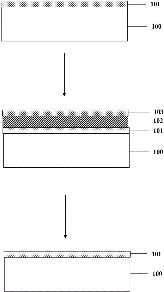
[0026] Step 1. Clean two GaN-based LED epitaxial wafers of the same batch, use acetone to ultrasonic for 5 minutes, boil with acetone, ethanol, and aqua regia in turn, wash with deionized water, and blow dry with nitrogen;

[0027] Step 2. Spin-coat photoresist on the surface of the epitaxial wafer, and use ICP etching technology to form a step structure to expose the n-GaN layer;

[0028] Step 3, PECVD deposition of SiO 2 , photolithography and etching with BOE to form SiO 2 barrier layer;

[0029] Step 4, sputtering a thin Ni layer with a thickness of 4-5nm on the surface as a catalytic layer;

[0030] Step 5. Put the epitaxial wafer into the CVD reaction chamber to grow graphene under the same conditions, the flow rate of argon gas is 960 sccm, the flow rate of hydrogen gas is 40 sccm, the flow rate of methane is 40 sccm, the growth temperature is 800°C, and the growth time is 5 minutes;

[0031] Step 6, growing 550nm Cu on the epitaxial wafer grown with graphene by magn...


PUM


Abstract

The invention provides a method for improving the quality of graphene directly grown on a nonmetal substrate, belonging to the field of growth of a semi-conducting material. The method comprises the following steps: growing a layer of a graphene film on the nonmetal substrate by using a chemical vapor deposition (CVD) method; then sputtering a thin metal layer on the graphene film; subjecting the substrate with the grown thin metal layer to CVD growth of the graphene film again; and after completion of growth, removing the surface graphene film and the metal layer. The method improves the quality of graphene directly grown on the nonmetal substrate; and after catalytic growth again, the quality and performance of the graphene film are substantially improved.

Description

Technical field: [0001] The invention relates to a method for improving the quality of graphene directly grown on a non-metallic substrate, and belongs to the technical field of semiconductor material growth. Background technique: [0002] In 2004, graphene was separated from graphite by scientists at the University of Manchester in the United Kingdom. Before that, graphene had been considered a hypothetical structure and could not exist stably alone. Graphene is a flat film with a hexagonal honeycomb structure composed of carbon atoms in sp2 hybrid orbitals. It is a two-dimensional material with a thickness of only one carbon atom (about 0.335nm). As the thinnest and hardest material in the world, graphene has many excellent properties that other materials do not have: the electron mobility exceeds 15000 cm at room temperature 2 / V·S, the resistivity is only 10 -6 Ω·cm, lower than copper or silver; the transmittance of single-layer graphene to visible light reaches 97.7%,...

Claims


Application Information

Patent Timeline
IPC IPC(8): C01B31/04
CPCC01P2002/82
Inventor 孙捷樊星许坤郭伟玲徐晨邓军
Owner BEIJING UNIV OF TECH
Why Eureka
Try Eureka