Anti-fuse memory cell

A memory unit and antifuse technology, applied in static memory, read-only memory, information storage, etc., can solve problems of manufacturability and reliability, high voltage exposure of MOS switching elements, doubtful manufacturability, etc.

Active Publication Date: 2016-08-10
SYNOPSYS INC
View PDF27 Cites 13 Cited by
  • Summary
  • Abstract
  • Description
  • Claims
  • Application Information

AI Technical Summary

Problems solved by technology

[0020] Although Peng implemented a cross-point memory structure, his array required CMOS process modifications (LDD elimination, thicker gate oxide at the edges) and had the following disadvantages: (a) all row decoders, column decoders Detectors and sense amplifiers must switch over a wide voltage range of 8V / 3.3V / 0V or 8V / 1.8V / 0V
[0024] All prior art antifuse cells and arrays either require special processing steps or have issues with high voltage exposure of the MOS switching elements, causing manufacturability and reliability issues
They are also limited to low-density memory applications (except for Peng's single-transistor cells), which in turn has very questionable manufacturability

Method used


Image

  • Anti-fuse memory cell
  • Anti-fuse memory cell
  • Anti-fuse memory cell

Examples


Embodiment Construction

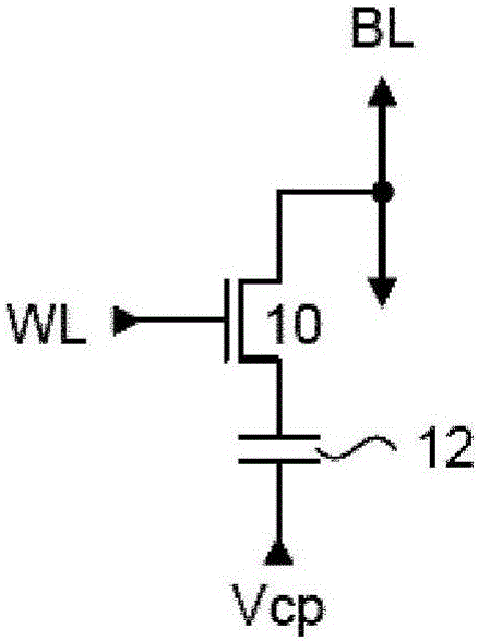
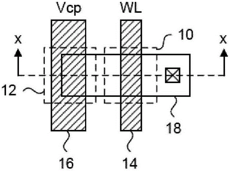
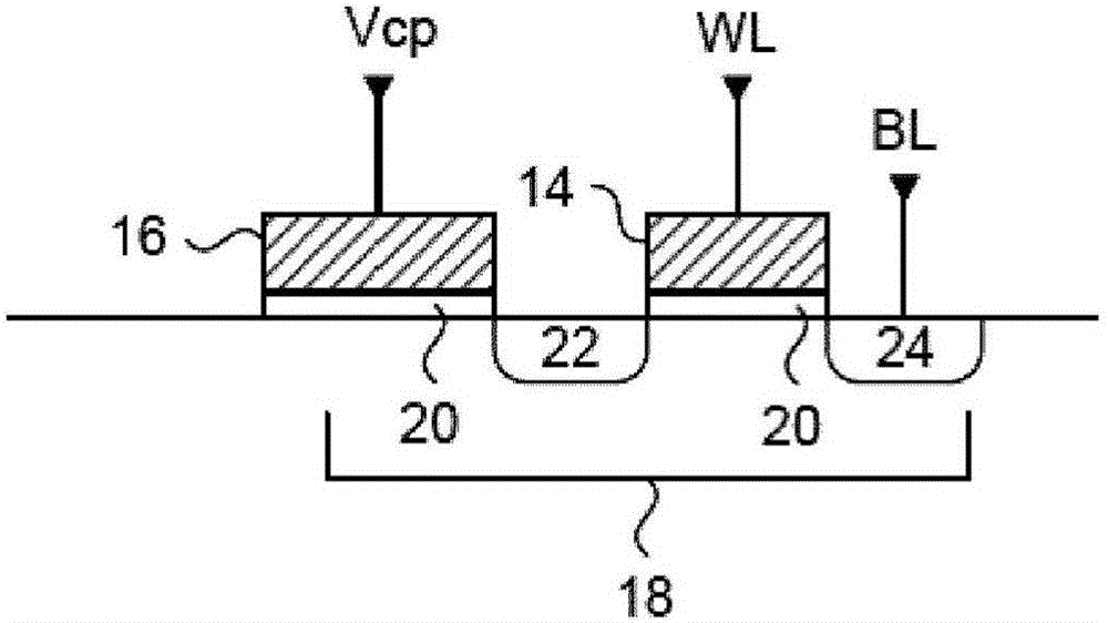
[0059] The present invention generally provides a variable thickness gate oxide antifuse transistor device useful for non-transitory one-time programmable (OTP) memory array applications. The antifuse transistor can be fabricated in standard CMOS technology and configured as a standard transistor element with source diffusion, gate oxide and polysilicon gate. The variable gate oxide under the polysilicon gate consists of a thick gate oxide region and a thin gate oxide region, where the thin gate oxide region acts as a local breakdown voltage region. A conductive path between the polysilicon gate and the channel region may be formed in the local breakdown voltage region during a programming operation. In memory array applications, the word line read current applied to the polysilicon gate can be sensed through the channel of the antifuse transistor through the bit line connected to the source diffusion. More specifically, the present invention provides an efficient method of u...


PUM


Abstract

An anti-fuse memory cell having a variable thickness gate oxide. The variable thickness gate oxide is formed by depositing a first oxide over a channel region of the anti-fuse memory cell, removing the first oxide in a thin oxide area of the channel region, and then thermally growing a second oxide in the thin oxide area. The remaining first oxide defines a thick oxide area of the channel region. The second oxide growth occurs under the remaining first oxide, but at a rate less than thermal oxide growth in the thin oxide area. This results in a combined thickness of the first oxide and the second oxide in the thick oxide area being greater than second oxide in the thin oxide area.

Description

technical field [0001] The present invention generally relates to non-volatile memory. More specifically, the present invention relates to antifuse memory cell structures. Background technique [0002] Over the past 30 years, antifuse technology has attracted a great deal of attention from inventors, integrated circuit designers and manufacturers. An antifuse is a structure that can change to a conducting state, or in other words, an electronic device that changes from a non-conducting to a conducting state. Equivalently, the binary state can be one of high and low resistance in response to electrical stress, such as a programming voltage or current. There have been many attempts to develop and apply antifuses in the microelectronics industry, but the most successful applications of antifuses to date can be seen in Field Programmable Gate Array (FGPA) devices made by Actel and Quicklogic, and in DRAM devices by Micron. Redundancy or option programming used in access memor...

Claims


Application Information

Patent Timeline
Patent Type & Authority Applications(China)
IPC IPC(8): H01L21/02G11C17/16H01L21/316H01L21/8247H01L27/115
CPCG11C17/16H01L21/823462H01L23/5252H10B20/20
Inventor 沃德克·库尔贾诺韦茨
Owner SYNOPSYS INC
Why Eureka
Try Eureka