Growth method for current expansion layer and LED epitaxial structure comprising current expansion layer

A technology of a current spreading layer and a growth method, applied in the field of LED epitaxial structure, can solve the problems of current crowding, low luminous efficiency, and high resistance of the N layer, and achieve uniform current distribution, simplified process flow, and convenient parameter control. Effect

Active Publication Date: 2016-08-17
XIANGNENG HUALEI OPTOELECTRONICS
View PDF4 Cites 2 Cited by
  • Summary
  • Abstract
  • Description
  • Claims
  • Application Information

AI Technical Summary

Problems solved by technology

[0013] The current distribution of the N layer of the existing LED epitaxial growth is uneven, which leads to the current crowding and the high resistance of the N layer, resulting in uneven current distribution of the light-emitting layer and low luminous efficiency.

Method used


Image

  • Growth method for current expansion layer and LED epitaxial structure comprising current expansion layer
  • Growth method for current expansion layer and LED epitaxial structure comprising current expansion layer
  • Growth method for current expansion layer and LED epitaxial structure comprising current expansion layer

Examples


Embodiment 1

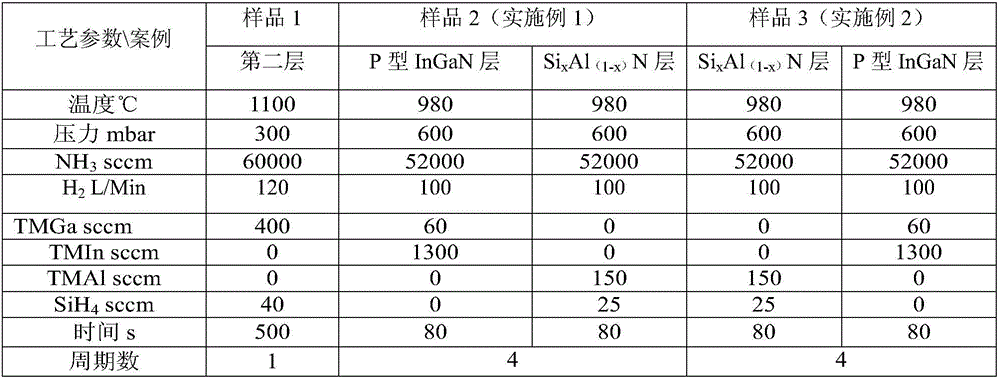
[0048] Use MOCVD to grow high-brightness GaN-based LED epitaxial wafers, specifically: use high-purity H 2 or high purity N 2 or high purity H 2 and high purity N 2 The mixed gas as the carrier gas, high-purity NH 3 As the N source, the metal-organic source trimethylgallium (TMGa) is used as the gallium source, trimethylindium (TMIn) is used as the indium source, and the N-type dopant is silane (SiH 4 ), trimethylaluminum (TMAl) as the aluminum source P-type dopant is dimagnesocene (CP 2 Mg), the substrate is sapphire, and the reaction pressure is between 70mbar and 900mbar.

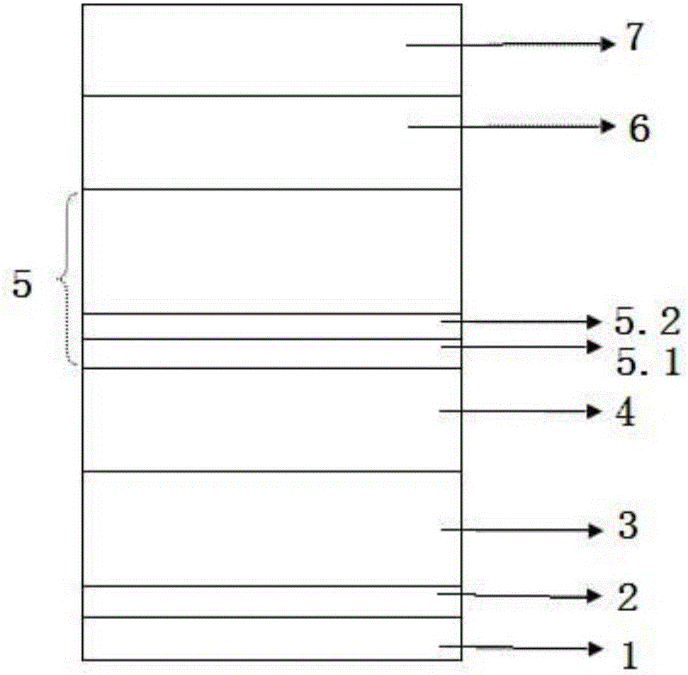
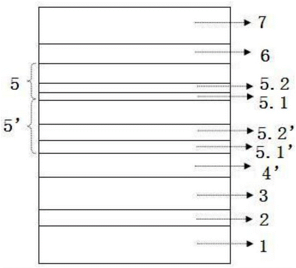
[0049] An LED epitaxial structure, see figure 2 , including the following structure: from bottom to top, it includes a sapphire substrate 1, a low-temperature buffer layer 2, an undoped GaN buffer layer 3, a Si-doped N-type GaN single layer 4', a current spreading layer 5', a light emitting layer 5, p-type AlGaN layer 6 and p-type GaN layer 7 doped with magnesium;

[0050] The thickness of the lo...

Embodiment 2

[0071] The only difference from Embodiment 1 is that the current spreading layer 5' includes four individual pieces, and the individual pieces include Si from bottom to top. x Al (1-x) N and P-type InGaN layers, where x=0.20.

Embodiment 3

[0073] The only difference from Embodiment 1 is that the current spreading layer 5' comprises 8 single pieces.


PUM


Abstract

The invention discloses a growth method for a current expansion layer. The growth method comprises a step of periodically growing 4-10 single pieces, wherein each single piece comprises a P type InGaN layer and an Si<x>Al<(1-x)>N layer or the Si<x>Al<(1-x)>N layer and the P type InGaN layer from the bottom up in sequence. The invention also discloses an LED epitaxial structure comprising the current expansion layer. By adoption of the current expansion layer, the rapid propagation of electrons from the N layer to the light emitting layer can be blocked by taking the high energy band of the GaN as the barrier; the longitudinally-propagated and relatively-crowded electrons can be transversely dispersed in a proper degree under the blocking of the energy band of the GaN; meanwhile, high-concentration two-dimensional electron gas is formed by the current expansion layer; the transverse mobility of the two-dimensional electron gas is quite high, so that the transverse expansion of the electrons is accelerated; the current is effectively expanded when the current passes through the current expansion layer macroscopically; and then the current distribution of the light emitting layer becomes uniform, so that the various kinds of performances of the LED are improved.

Description

technical field [0001] The invention relates to the technical field of LEDs, in particular to a method for growing a current spreading layer and an LED epitaxial structure containing the structure. Background technique [0002] At present, LED is a kind of solid-state lighting, which has the advantages of small size, low power consumption, long service life, high brightness, environmental protection, durability, etc., and is deeply loved by consumers. With the gradual expansion of the scale of domestic production of LEDs, the demand for LED light effects in the market is increasing day by day. [0003] The growth method of existing LED epitaxial structure (its structure is detailed in figure 1 ) includes the following steps: [0004] The first step, under the hydrogen atmosphere of 1000-1100 ℃, pass 100-130L / min of H 2 , keep the reaction chamber pressure 100-300mbar (air pressure unit), process the sapphire substrate 1, and the processing time is 5-10 minutes; [0005] ...

Claims


Application Information

Patent Timeline
Patent Type & Authority Applications(China)
IPC IPC(8): H01L33/14H01L33/04H01L33/32H01L33/00
CPCH01L33/0075H01L33/04H01L33/14H01L33/32
Inventor 徐平
Owner XIANGNENG HUALEI OPTOELECTRONICS
Why Eureka
Try Eureka