
Graphene Photodetectors

A photodetector and graphene technology, applied in the field of photoelectric detection, can solve the problem of low response rate, and achieve the effects of fast response time, excellent light sensitivity, and compatible preparation technology

Active Publication Date: 2017-06-30
泰州巨纳新能源有限公司
View PDF12 Cites 0 Cited by
  • Summary
  • Abstract
  • Description
  • Claims
  • Application Information

AI Technical Summary

Problems solved by technology

However, this mechanism has a great limitation, that is, the charge transfer and / or charge trapping process existing in photoelectric conversion, resulting in an extremely low response rate, in milliseconds, or even more than seconds

Method used


Image

  • Graphene Photodetectors

Examples


Embodiment 1

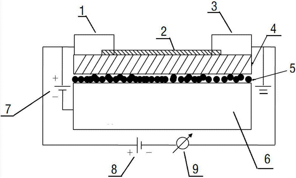
[0023] A graphene photodetector, the main structure of the detector includes single-layer graphene (prepared by tearing tape method); 90nm silicon dioxide is deposited as an insulating medium layer by thermal evaporation; silicon is used as a gate electrode; a layer of CdSe semiconductor Quantum dots, as light-absorbing carriers, are deposited on the silicon surface by spin coating; gold / nickel, as source and drain electrodes, are connected to external circuits with a thickness of 50nm / 5nm, deposited by electron beam lithography and thermal evaporation. The response time of the photodetector in the near-infrared band reaches the nanosecond level, and the responsivity reaches 1.1×10 8 A / W, the response wavelength ranges from visible to near-infrared bands.

Embodiment 2

[0025] A graphene photodetector, the main structure of the detector comprises single-layer graphene (prepared by chemical vapor deposition); 120nm Al 2 o 3 As an insulating dielectric layer, it is deposited by thermal evaporation; Ge is used as a gate electrode; two layers of PbS semiconductor quantum dots, as a light-absorbing carrier, are deposited on the surface of Ge by spin coating; gold / nickel is used as a source and drain, connected to an external circuit , with a thickness of 50nm / 5nm, deposited by electron beam lithography and thermal evaporation. The response time of the photodetector in the near-infrared band reaches the nanosecond level, and the responsivity reaches 1.2×10 8 A / W, the response wavelength ranges from visible to near-infrared bands.

Embodiment 3

[0027] A graphene photodetector, the main structure of the detector includes two layers of graphene (prepared by chemical vapor deposition); 100nm silicon dioxide is used as an insulating medium layer and deposited by thermal evaporation; Si is used as a gate electrode; four layers of CdS semiconductor Quantum dots, as light-absorbing carriers, are deposited on the Si surface by spin coating; gold / nickel, as the source and drain electrodes, are connected to external circuits with a thickness of 50nm / 5nm, deposited by electron beam lithography and thermal evaporation. The response time of the photodetector in the near-infrared band reaches the nanosecond level, and the responsivity reaches 1.35×10 8 A / W, the response wavelength ranges from visible to near-infrared bands.


PUM


Abstract

The invention discloses a graphene photoelectric detector. The structure of the detector sequentially comprises a gold / nickel layer, graphene, silicon dioxide, a semiconductor nanometer structure and a silicon substrate, wherein the gold / nickel layer is taken as a source and a drain which are connected with an external circuit, the graphene is taken as an electron transmission layer, the silicon dioxide is taken as an insulation dielectric layer, the semiconductor nanometer structure is taken a light absorption carrier, and the silicon substrate is taken as a grid electrode. The working wave band of the detector can be effectively controlled according to the types, the sizes and the like of the semiconductor nanometer structures, the detector simultaneously has excellent luminous sensitivity and fast response time, and the bottleneck of the graphene photoelectric detector in performance of ultra-high speed, super-sensitivity response and different demand response wave band ranges is successfully broken through. Further, the fabrication process of the detector is simple and is completely compatible with an existing silicon technology and a fabrication technology of the semiconductor nanometer structure.

Description

technical field [0001] The invention relates to the technical field of photoelectric detection, in particular to a graphene film-based photodetector. Background technique [0002] In 2004, graphene was first discovered by a research team led by Professor Andre Geim of the University of Manchester. It is the thinnest known material (only a single carbon atom layer thick), and has a very high carrier mobility (intrinsic mobility ~ 200,000cm 2 v -1 the s -1 ), very good low-dimensional stability, ultra-wide spectral absorption range, and electric field modulation of electron concentration, it is considered to be a very potential electronic / optoelectronic material, so it has extremely wide applications in many fields, For example, it can be used to prepare microelectronic devices such as high-performance field effect transistors, photoelectric devices such as solar cells, photodetectors (especially infrared light detection), etc. However, the zero-gap energy band structure o...

Claims


Application Information

Patent Timeline
Patent Type & Authority Patents(China)
IPC IPC(8): H01L31/112H01L31/0328B82Y30/00
CPCB82Y30/00H01L31/0328H01L31/112
Inventor 梁铮倪振华丁荣梁贺君陈谷一袁文军王阳晖
Owner 泰州巨纳新能源有限公司
Learn More