A method for self-organized nucleation and epitaxial gan materials on graphene

A graphene, self-organizing technology, applied in electrical components, semiconductor/solid-state device manufacturing, circuits, etc., can solve problems affecting the service life and efficiency of GaN-based devices, complex processes, etc., to improve crystal quality, improve Use efficiency and service life, the effect of strong practicality

Active Publication Date: 2018-08-31
THE 13TH RES INST OF CHINA ELECTRONICS TECH GRP CORP
View PDF3 Cites 0 Cited by
  • Summary
  • Abstract
  • Description
  • Claims
  • Application Information

AI Technical Summary

Problems solved by technology

However, this method has complex processes, and because the zinc oxide nanowall introduces oxygen impurities, forming a shallow buried charge layer, which in turn affects the service life and efficiency of gallium nitride-based devices on graphene.

Method used


Image

  • A method for self-organized nucleation and epitaxial gan materials on graphene
  • A method for self-organized nucleation and epitaxial gan materials on graphene

Examples


Embodiment Construction

[0022] The present invention will be further described in detail below in conjunction with the accompanying drawings and specific embodiments.

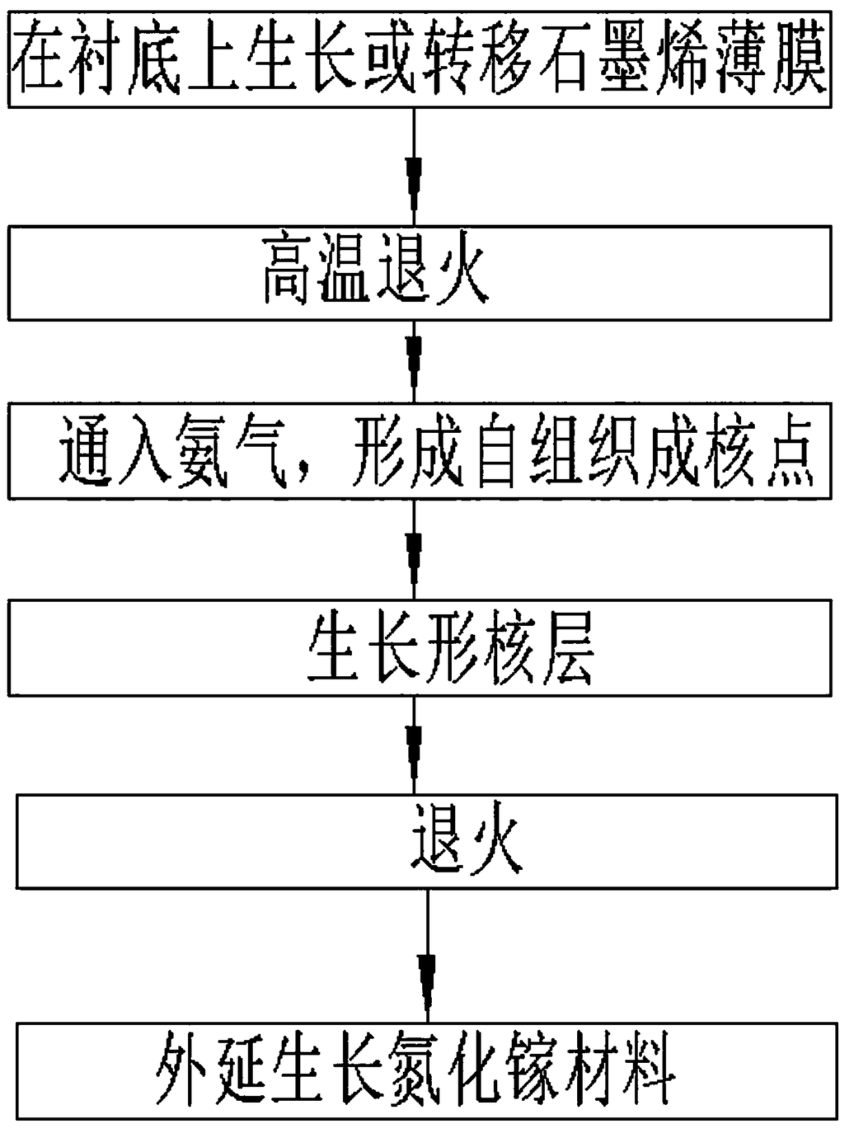
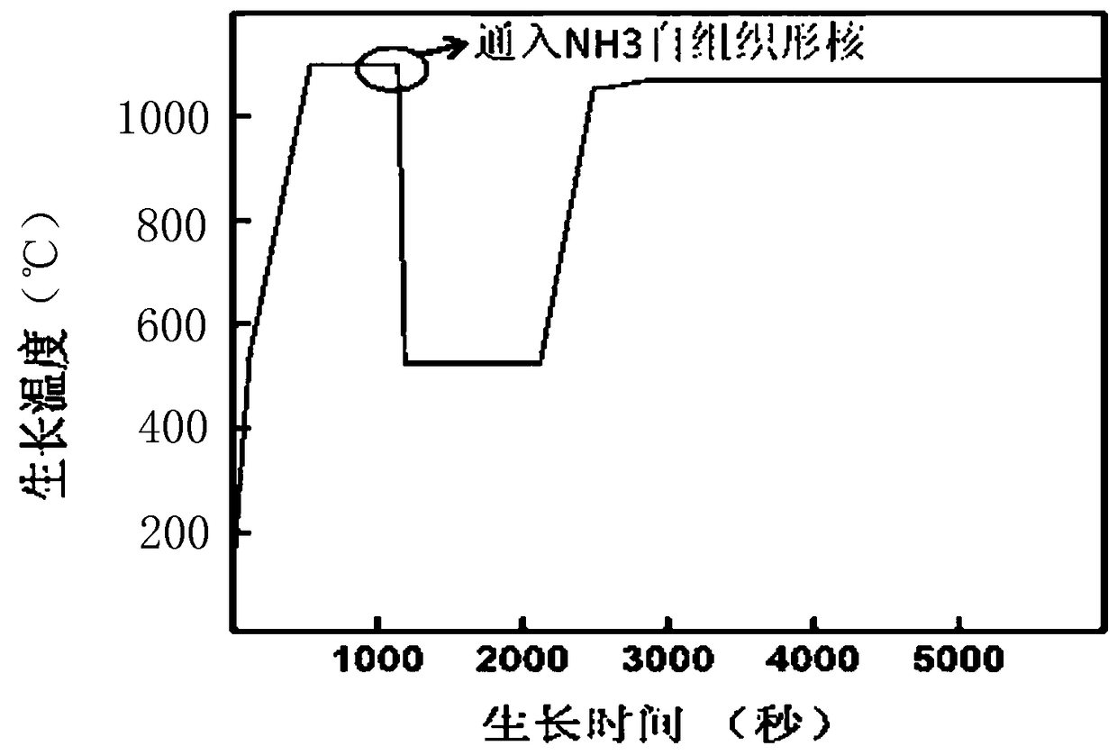
[0023] In the present invention, after high temperature annealing, NH 3 Etching graphene, introducing point defects into graphene, taking advantage of the low surface potential and high chemical activity of point defects, using point defects as nucleation points, regrowing nucleation layers, and forming self-organized nucleation nuclear layer. The present invention utilizes NH 3 The etching self-organization nucleation method to prepare GaN materials can effectively solve the problem of low nucleation density of GaN grown on graphene, improve the crystal quality of GaN materials on graphene, and has strong practicability. Concrete steps of the present invention are as follows:

[0024] Step 1, grow or transfer the graphene film on the substrate: use CVD technology to grow or transfer the graphene film on the substrate, use CH 4 As...


PUM

PropertyMeasurementUnit
thicknessaaaaaaaaaa

Abstract

The invention discloses a method for epitaxial growth of a GaN material on graphene through a self-organizing nucleating mode, and belongs to the technical field of the semiconductor. The method comprises the following steps of enabling a graphene thin film to be grown or transferred to a substrate; adopting an MOCVD technology, and carrying out high-temperature annealing in an MOCVD reaction chamber; pumping NH<3> to form self-organizing nucleating points on the graphene thin film; enabling a nucleating layer to be grown; annealing to realize nucleating layer crystallization; and carrying out epitaxial growth of the GaN material on the self-organizing nucleating layer after the temperature is changed. By adoption of the method, the nucleating points on the graphene can be increased, so that the formation of the nucleating layer on the graphene can be promoted; the crystal quality of the graphene gallium nitride material on the graphene can be further improved; and the use efficiency of the device is improved while the service life of the device is prolonged.

Description

technical field [0001] The invention belongs to the technical field of semiconductors, in particular to a method for self-organizing nucleation and epitaxial GaN material on graphene. Background technique [0002] As a typical representative of the third-generation semiconductor, gallium nitride materials are widely used in electronic systems such as wireless communication and radar in the microwave and millimeter wave frequency bands due to their wide band gap and high electron velocity. The development prospect of optoelectronics and microelectronics is very broad. [0003] Graphene is a two-dimensional honeycomb crystal film with closely arranged carbon atoms. This special layered structure of graphene makes it possible to have only intermolecular van der Waals force between it and gallium nitride, so it is easy to peel off and transfer, and it is convenient to transfer to On other substrates, such as glass and flexible substrates, it is of great significance to realize ...

Claims


Application Information

Patent Timeline
Patent Type & Authority Patents(China)
IPC IPC(8): H01L21/02
CPCH01L21/02376H01L21/02513H01L21/0254H01L21/0262H01L21/02658
Inventor 王波房玉龙尹甲运郭艳敏李佳芦伟立冯志红
Owner THE 13TH RES INST OF CHINA ELECTRONICS TECH GRP CORP
Why Eureka
Try Eureka