
Novel film bulk acoustic resonator and production method thereof

A thin-film bulk acoustic wave and resonator technology, which is applied in the direction of electrical components and impedance networks, can solve the problems that the film stress is difficult to control, the resonator has not been widely used, and the development is limited, so as to achieve the difficulty and complexity of the preparation process. Improve the mechanical strength and power capacity, which is beneficial to the effect of industrial production

Inactive Publication Date: 2016-09-21
UNIV OF ELECTRONIC SCI & TECH OF CHINA
View PDF6 Cites 20 Cited by
  • Summary
  • Abstract
  • Description
  • Claims
  • Application Information

AI Technical Summary

Problems solved by technology

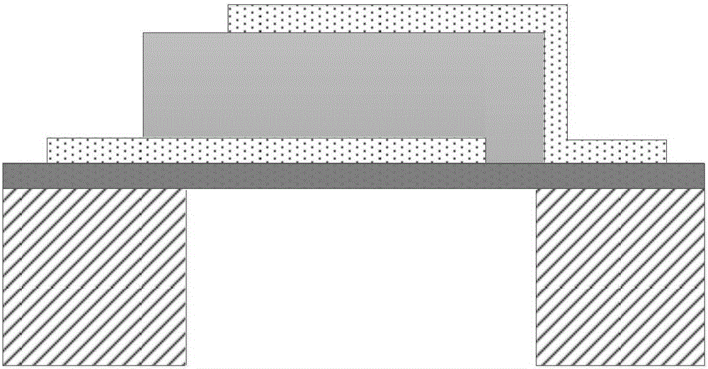
[0004] One is the silicon back etching type, and its structure is as follows figure 2 As shown, its working principle is that the sound wave is reflected on the interface between the bottom electrode or the support layer and the air; the structure hollows out the back of the silicon substrate to form an air interface, and a lot of resonators are required to prepare the filter. It will cause the hollowed-out area on the back of the substrate to be too large, which will greatly reduce the mechanical strength of the device, so this type of resonator has not been widely used;
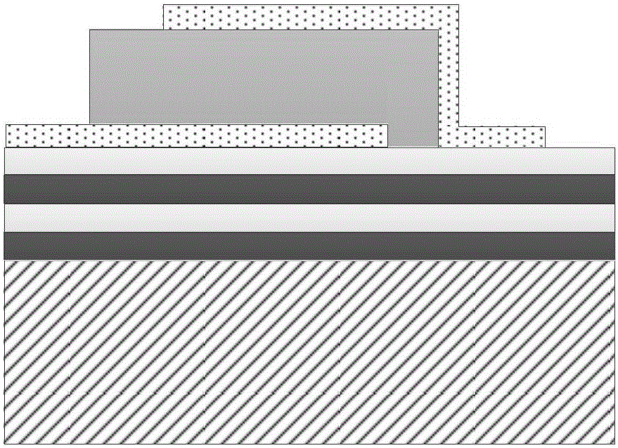
[0005] The second is the solid-state assembly type (SMR), and its structure is as follows image 3 As shown, its working principle is that the high acoustic impedance layer and the low acoustic impedance layer form a reflective layer to realize the reflection of sound waves. The thickness of each layer of material is 1 / 4 of the wavelength of the sound wave when it propagates in the material; The back-etched resonator has good mechanical strength and power capacity, and can be applied under high-power conditions, but the Bragg reflection layer of the SMR resonator needs to be precise for each layer of film in order to achieve the ideal sound wave reflection effect. In order to control the thickness, stress and roughness of the film, it is generally necessary to perform CMP processing on each layer of the film to ensure that its roughness meets the requirements of the device, resulting in a complicated manufacturing process and high manufacturing cost for the SMR device;
[0006] The third is the air-gap type (FBAR), and its structure is as follows Figure 4 As shown, its working principle is that the sound wave is reflected at the interface between the bottom electrode or the support layer and the air; the structural resonator has high sound wave reflection efficiency, high Q value, low insertion loss, and easy integration, etc., and is the most widely used , but in the process of preparing the cavity of the FBAR resonator, the stress of the film is difficult to control, which often causes the failure of the entire device and limits the product yield, and the formation of a perfect cavity requires a very high level of technology
[0007] In summary, the existing thin-film bulk acoustic resonators are all complicated and difficult to prepare, resulting in high manufacturing costs and low product qualification rates, which greatly limit the development of the entire industry

Method used


Image

  • Novel film bulk acoustic resonator and production method thereof
  • Novel film bulk acoustic resonator and production method thereof
  • Novel film bulk acoustic resonator and production method thereof

Examples


Embodiment Construction

[0035] The present invention will be described in further detail below in conjunction with the accompanying drawings and embodiments, but it should be noted that the present invention is not limited to the embodiments.

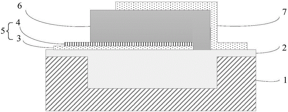
[0036] This embodiment provides a thin film bulk acoustic resonator, the structure of which is as follows figure 1 As shown, the substrate 1 including the preset groove is fully filled with the low acoustic impedance layer 2 in the groove and evenly covers the upper surface of the substrate, and the high conductivity electrode layer 3 and the high acoustic impedance layer 2 are sequentially arranged on the low acoustic impedance layer 2. The impedance electrode layer 4 together constitutes a composite bottom electrode 5, on which a piezoelectric layer 6 and a top electrode 7 are sequentially arranged.

[0037] In this embodiment, the substrate adopts a silicon substrate with a crystal orientation with a silicon dioxide layer; the low acoustic impedance layer...


PUM

PropertyMeasurementUnit
Thicknessaaaaaaaaaa

Abstract

The invention belongs to the radio frequency micro-electromechanical system technology field, to be specific, provides a novel film bulk acoustic resonator and a production method thereof. The film bulk acoustic resonator comprises a substrate; a bottom electrode, a piezoelectric layer, and a top electrode, which are sequentially disposed on the substrate. The substrate is provided with a groove, and a low acoustic impedance layer is disposed on the upper surface of the substrate and in the groove, and in addition, the bottom electrode, the piezoelectric layer, and the top electrode are disposed on the low acoustic impedance layer. The bottom electrode is the composite bottom electrode formed by sequentially arranging a high-conductivity electrode layer and a high acoustic impedance electrode layer in a laminated on the low acoustic impedance layer. The novel film bulk acoustic resonator and the production method thereof are advantageous in that the performance of the resonator is excellent, and the production technology difficulty and the complexity are greatly reduced; the production yield of the film bulk acoustic resonant is obviously improved, the production cost is greatly reduced, and the production period is shortened; the industrialized production is facilitated, and great meaning is provided for broadening the application field.

Description

technical field [0001] The invention belongs to the technical field of radio frequency micro-electromechanical systems, and in particular relates to a novel film bulk acoustic wave resonator and a preparation method thereof. Background technique [0002] Thin film bulk acoustic resonator is a component based on piezoelectric technology. The size of the resonator is extremely small, which is 4 to 5 orders of magnitude smaller than that of components that only use electromagnetic waves as propagation signals; the insertion loss is small, and the Q value is high. It can reach more than 1000; the operating frequency is high, and the withstand power capacity is larger than that of the surface acoustic wave device; and it can be compatible with the CMOS process. In view of the above advantages, the thin film bulk acoustic resonator technology has quickly occupied the radio frequency communication market. Biochemical detection, ultraviolet detection, etc. also have broad applicatio...

Claims


Application Information

Patent Timeline
IPC IPC(8): H03H3/02H03H9/02H03H9/05H03H9/17
CPCH03H3/02H03H9/02015H03H9/0509H03H9/173H03H2003/021H03H2003/023
Inventor 钟慧霍振选张睿秦康宁杨泰张根石玉
Owner UNIV OF ELECTRONIC SCI & TECH OF CHINA
Learn More